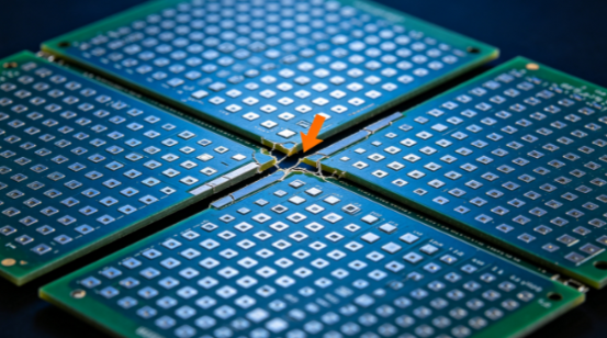
In fine-pitch PCB assembly, the solder mask bridge between adjacent pads can become one of the weakest structural features on the board. This is particularly important for BGA packages with very small pad spacing, where the available solder mask bridge width may be only a few tens of micrometers.
When a bridge lifts, cracks, or separates from the copper surface, the failure is not necessarily caused by an incorrect PCB layout. In many cases, it results from the combined effects of material properties, thermal stress, copper surface condition, solder mask geometry, and manufacturing processes.
For this reason, PCB design rules alone are not always sufficient to predict solder mask reliability. The interaction between design, materials, and process capability must also be considered.
Two Main Mechanisms Behind Solder Mask Bridge Failure
There are two major mechanisms that should be considered when investigating a cracked or delaminated solder mask bridge.
1. CTE Mismatch Increases Local Thermal Stress
Different materials in a PCB have different coefficients of thermal expansion (CTE). FR-4 laminate, copper, surface-finish layers, and cured solder mask do not expand or contract at the same rate during reflow.
When a PCB is heated to soldering temperatures and subsequently cooled to room temperature, these differences in expansion create mechanical strain.
A simplified relationship is:
Thermal strain ≈ ΔCTE × ΔT
However, this equation provides only a first-order estimate. The actual stress in a solder mask bridge also depends on elastic modulus, thickness, geometry, adhesion, cure condition, copper pattern density, and mechanical constraints.
The problem becomes more significant when the distance between adjacent pads is very small. A narrow solder mask bridge has less cross-sectional area and therefore less mechanical margin. Stress can become concentrated near the bridge root, especially around sharp corners or irregular copper edges.
This means that CTE mismatch should be evaluated together with bridge geometry rather than being treated as an independent failure factor.

2. Interface Adhesion Can Fail Before the Solder Mask Bulk Material
A solder mask bridge can fail through cohesive cracking within the solder mask or adhesive/interface failure between the solder mask and copper.
For dense BGA layouts, the second mechanism can be particularly difficult to identify.
During exposure, development, baking, and final curing, the solder mask undergoes chemical and dimensional changes. If the bridge is extremely narrow, small variations in exposure energy, development, copper surface morphology, and curing can significantly affect its effective cross-section and adhesion.
The interface between the solder mask and copper should therefore be considered a critical reliability region.
Important factors include:
- Copper surface roughness
- Copper cleanliness
- Surface treatment chemistry
- Solder mask formulation
- Exposure and development conditions
- Final curing conditions
- Moisture absorption
- Thermal history
- Local copper geometry
A narrow bridge that already has poor adhesion before reflow may crack or lift when exposed to repeated thermal expansion and contraction.
Why Fine-Pitch BGA Pads Are More Difficult
BGA layouts with small pad spacing create several simultaneous manufacturing challenges.
First, the available space for the solder mask bridge becomes very limited. Second, small dimensional variations can represent a significant percentage of the bridge width.
For example, if the nominal bridge width is only 60–70 μm, a relatively small process variation can substantially change its remaining cross-sectional area.
The problem can become more complicated when solder-mask registration, copper-pad size, surface finish, and exposure compensation are considered together.
Therefore, BGA solder mask design should not be evaluated only from the nominal CAD dimensions. Engineers should also consider:
- Actual pad-to-pad spacing
- Solder mask registration tolerance
- Copper etching tolerance
- Surface-finish thickness
- Exposure compensation
- Development capability
- Minimum reliable bridge width
- Supplier process capability
A design that is theoretically manufacturable may still have insufficient process margin for stable mass production.
Copper Surface Roughness and Solder Mask Adhesion
Copper surface condition has a direct influence on solder mask adhesion.
Some degree of surface treatment or roughening is commonly used to improve mechanical bonding. However, excessive roughness is not automatically beneficial.
Very rough copper surfaces can contain sharp peaks and valleys that increase local stress concentration. They can also affect solder-mask coating uniformity and the geometry of extremely narrow bridges.
Therefore, solder mask adhesion should be evaluated together with copper surface morphology.
The appropriate roughness range depends on the copper foil, surface-treatment process, solder mask system, and manufacturer capability. Rather than applying a universal Rz value to every PCB, engineers should use the solder-mask supplier’s process window and validate it through adhesion and thermal-reliability testing.
Surface Finish Also Matters
ENIG and OSP can produce different surface conditions beneath the solder mask.
With ENIG, the copper is covered by an electroless nickel layer and a thin immersion-gold layer. The surface-finish thickness and edge geometry can influence the remaining solder-mask bridge width, particularly in extremely dense pad patterns.
With OSP, the copper surface is protected by an organic coating. Surface cleanliness, pretreatment, coating uniformity, and storage conditions can influence the subsequent solder-mask adhesion process.
This does not mean that ENIG or OSP is inherently unsuitable for fine-pitch BGA applications. Instead, the solder-mask process must be compatible with the selected PCB surface finish.
A robust process should verify the complete sequence:
Copper preparation → solder mask coating → exposure → development → curing → surface finishing → assembly
Changing one step without evaluating the entire process chain can reduce the available reliability margin.
Solder Mask Thickness and Bridge Geometry
Bridge reliability depends on more than bridge width.
Other geometric parameters include:
- Solder mask thickness
- Bridge height
- Pad spacing
- Pad shape
- Copper edge profile
- Mask-to-pad registration
- Corner geometry
- Local copper density
An extremely narrow but relatively thick solder mask bridge can behave differently from a wider, thinner bridge.
For this reason, the phrase “smaller bridge means higher density” should not automatically be interpreted as better PCB design.
The practical objective is to achieve the smallest bridge that remains within the manufacturer’s stable process capability.
Post-Cure and Moisture Management
Curing conditions can strongly influence solder-mask mechanical properties and adhesion.
Insufficient curing may leave residual solvents or incomplete polymerization, while excessive or poorly controlled thermal treatment can change the material’s mechanical behavior.
Moisture is another important consideration. PCB materials can absorb moisture during storage and handling. During subsequent heating, absorbed moisture can contribute to interfacial stress or other assembly-related reliability problems.
For this reason, PCB manufacturing controls should include appropriate:
- Solder mask curing
- Moisture management
- Pre-assembly storage
- Baking requirements when applicable
- Surface preparation
- Process monitoring
The correct cure profile should be established according to the solder-mask manufacturer’s technical data and the actual PCB construction rather than using one temperature/time combination for every product.
Why Design Rules Alone Are Not Enough
A common mistake is to treat IPC design guidance as a guarantee that a solder mask bridge will survive production.
Design standards provide important manufacturing and reliability guidance, but they do not eliminate process variation.
For dense BGA layouts, the actual production result is affected by:
CAD geometry + material system + manufacturing tolerance + process capability + assembly thermal profile
A bridge that satisfies a nominal design rule may still be vulnerable if the manufacturer cannot consistently control registration, exposure, development, curing, or copper surface preparation.
Therefore, PCB manufacturing capability should be reviewed at the beginning of the design process, not only after the PCB enters production.
Practical Design Rules for Fine-Pitch BGA
There is no single universal minimum solder-mask bridge width that is appropriate for every PCB manufacturer.
Instead, the recommended design value should be established from the supplier’s demonstrated process capability.
For fine-pitch BGA designs, engineers should review:
- Minimum pad-to-pad spacing
- Minimum solder-mask bridge width
- Registration tolerance
- Copper surface condition
- Solder-mask thickness
- Surface-finish compatibility
- Cure profile
- Thermal-cycle requirements
- Expected production volume
- Supplier process capability
If the required bridge width is close to the manufacturer’s lower process limit, alternative pad strategies such as NSMD may need to be considered.
However, changing to NSMD should also be evaluated for solder-joint geometry, package recommendations, pad definition, solder-mask registration, and assembly reliability.
Common Failure Modes That Can Be Misidentified
A broken solder-mask bridge does not always indicate solder-mask adhesion failure.
Several other defects can produce similar visual symptoms:
- Copper-pad lifting
- Solder-mask cracking
- Surface contamination
- Incomplete curing
- Excessive solder-mask registration error
- Copper surface oxidation
- Lamination-related delamination
- Mechanical damage during depanelization
- Thermal damage during reflow
Therefore, failure analysis should begin with cross-sectional inspection rather than assuming a single mechanism.
Optical microscopy can identify obvious bridge cracks and lifting. Cross-section analysis can determine whether the failure originates in the solder mask, copper interface, laminate, or another structural region.
SEM and elemental analysis may be used when the failure mechanism cannot be established through conventional metallography.
A Practical Verification Workflow at Kingda
For dense BGA and high-density PCB projects, PCB reliability should be evaluated before mass production.
Kingda recommends a structured verification workflow.
Step 1: Review the PCB Layout
Identify areas where pad spacing is particularly small and calculate the actual solder-mask bridge width after considering registration tolerances.
Step 2: Review Material Compatibility
Check the compatibility between the solder mask, copper foil, surface finish, laminate, and assembly process.
Step 3: Verify Copper Surface Preparation
Confirm that copper cleanliness, surface treatment, and roughness are within the solder-mask supplier’s recommended process window.
Step 4: Verify Exposure and Development
Inspect the bridge profile under magnification and confirm that narrow features are reproduced consistently.
Step 5: Verify Final Curing
Check the solder-mask cure profile and ensure that the actual production process follows the material supplier’s requirements.
Step 6: Conduct Cross-Section Analysis
For high-risk BGA regions, cross-section samples can reveal:
- Actual bridge width
- Mask thickness
- Interface condition
- Copper profile
- Registration accuracy
- Local defects
Step 7: Validate Through Assembly Testing
Representative reflow cycles, thermal cycling, and mechanical testing can be used when required by the product’s reliability specification.
The objective is not simply to prove that one prototype survived. It is to establish a repeatable process window for mass production.
Key Points for Engineers
When a fine-pitch BGA solder mask bridge fails, the correct troubleshooting sequence should be:
Geometry → Material → Interface → Process → Assembly → Reliability
Do not immediately assume that the CAD design is wrong.
At the same time, do not assume that compliance with a design standard guarantees reliability.
The most important questions are:
- Is the actual bridge width within the manufacturer’s capability?
- Is solder-mask registration stable?
- Is the copper surface suitable for adhesion?
- Is the solder mask fully cured?
- Is moisture properly controlled?
- Does the surface finish affect the available bridge geometry?
- Does the assembly thermal profile introduce excessive stress?
- Has the design been validated under representative production conditions?
Conclusion
Solder mask bridges in dense BGA areas are small structures with relatively limited mechanical margin. Their reliability is affected by CTE mismatch, interface adhesion, copper surface morphology, solder-mask geometry, curing conditions, surface finish, and assembly thermal history.
The key lesson is that a narrow solder-mask bridge should not be judged solely by its nominal CAD width. BGA solder mask reliability depends on the complete material and manufacturing system.
For high-density and fine-pitch PCB projects, Kingda recommends combining PCB design, material selection, process-capability review, cross-sectional inspection, and PCB reliability validation. By controlling the complete process chain rather than relying on a single dimensional rule, engineers can improve solder-mask bridge stability and reduce unexpected failures during reflow and mass production.