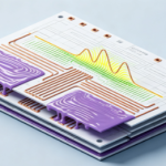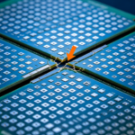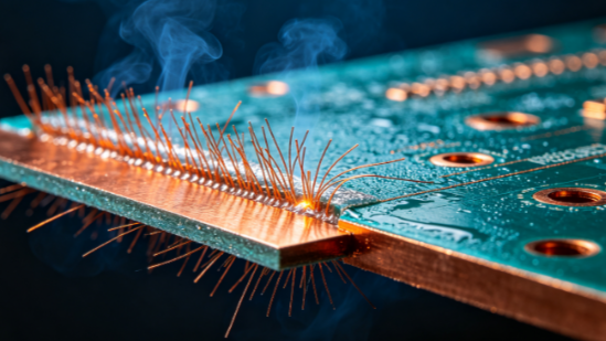
Copper whisker growth is an easily overlooked reliability issue in advanced PCB manufacturing, particularly in thin-copper, fine-pitch, and high-density BGA applications. Unlike conventional surface oxidation or ionic migration, copper whiskers are filament-like metallic structures that can develop from a copper surface under specific stress and microstructural conditions. If they extend toward adjacent conductors or solder joints, they may create unexpected mechanical interference or electrical failure paths.
For high-reliability PCB designs, understanding the relationship between copper foil structure, residual stress, lamination conditions, thermal cycling, and surface morphology is therefore important.
What Is Copper Whisker Growth?
Copper whisker growth refers to the formation and extension of fine, filament-like copper crystals from a copper surface. The phenomenon is generally associated with localized stress, defects, grain structure, recrystallization, and diffusion processes within the copper layer.
It should not simply be described as copper “growing hair.” A whisker is a crystallographically oriented metallic structure whose formation is influenced by the internal stress state and microstructure of the copper.
In multilayer PCBs, residual stress can be introduced during copper foil manufacturing, lamination, thermal processing, plating, and subsequent assembly. Differences in the coefficient of thermal expansion between copper, resin, glass fabric, and other materials can further modify the stress state during heating and cooling.
A simplified relationship is:
Thermal strain ≈ ΔCTE × ΔT
However, this does not mean that a specific CTE mismatch automatically produces whiskers. Actual whisker formation depends on the copper’s grain structure, residual stress, surface condition, thickness, processing history, defects, and thermal-mechanical environment.
Why Thin Copper Foil Requires Special Attention
Copper thickness is one of the factors that should be evaluated when investigating whisker formation.
Very thin copper foil has a relatively small cross-sectional volume and can be more sensitive to localized stress and microstructural changes. However, copper thickness alone cannot be used as a universal criterion for predicting whisker growth.
The risk may also be affected by:
- Copper grain orientation and grain size
- Residual tensile or compressive stress
- Surface roughness and morphology
- Manufacturing defects and inclusions
- Annealing and thermal history
- Lamination pressure and temperature
- Copper foil type and production process
- Subsequent soldering and reflow cycles
- Mechanical constraints imposed by the PCB stackup
Therefore, a statement such as “all copper below a certain thickness will form whiskers” is not technically appropriate. The correct approach is to evaluate copper foil thickness together with material structure and process conditions.
RA, ED, and HVLP Copper Foil: Why Microstructure Matters
Copper foil used in PCB manufacturing can have significantly different microstructures depending on how it is produced and treated. RA copper, ED copper, and HVLP copper should therefore not be evaluated solely according to nominal thickness.
RA, or rolled-annealed copper, is produced through mechanical rolling and annealing. Its grain structure and mechanical properties can differ substantially from those of electrodeposited copper.
ED copper is produced through an electrodeposition process. Its grain structure, texture, surface treatment, and mechanical properties depend strongly on the manufacturing process.
HVLP copper is characterized primarily by a low-profile copper surface, which is widely used to reduce conductor loss and improve high-speed signal performance. Its relevance to whisker behavior should be evaluated together with its grain structure, stress state, and surface treatment rather than simply assuming that lower roughness automatically eliminates whisker formation.
For this reason, a material comparison should consider:
| Factor | RA Copper | ED Copper | HVLP Copper |
|---|---|---|---|
| Manufacturing method | Rolled and annealed | Electrodeposited | Typically low-profile treated copper |
| Grain structure | Rolling-dependent | Deposition-dependent | Supplier/process-dependent |
| Surface profile | Application-dependent | Application-dependent | Low-profile surface |
| Mechanical behavior | Strongly influenced by annealing | Strongly influenced by deposition | Depends on foil construction |
| Whisker risk | Requires process validation | Requires process validation | Requires process validation |
| High-speed application | Application-dependent | Widely used | Particularly useful for low-loss designs |
This comparison demonstrates why copper foil selection should not be reduced to a simple ranking. Copper foil selection must be based on electrical requirements, mechanical reliability, manufacturing capability, and validated material data.
Residual Stress Is a Key Driver
The most important mechanism behind many whisker-growth phenomena is stress-driven atomic movement.
During PCB lamination, copper and dielectric materials experience different thermal expansion and contraction. As the laminated structure cools, the materials cannot always return to their original dimensions independently. Mechanical constraints can therefore create residual stress at interfaces and within the copper layer.
At a simplified level, stress can influence atomic diffusion and dislocation movement. Under suitable conditions, copper atoms can migrate toward energetically favorable locations, allowing a filamentary crystal structure to develop.
The process can be influenced by:
- Residual stress inside the copper layer
- Local stress concentration around surface defects
- Grain boundaries and crystallographic orientation
- Dislocation density
- Thermal cycling
- Copper surface morphology
- Mechanical constraints from the surrounding dielectric structure
Consequently, residual stress should be treated as an important investigation parameter rather than assuming that humidity, halogens, or electrical fields are always required.
The Role of Lamination and Cooling
Lamination conditions can significantly affect the final stress state of a multilayer PCB.
During the lamination cycle, the prepreg softens, resin flows, and copper foil becomes mechanically constrained within the multilayer structure. During cooling, differences in thermal expansion between copper and the dielectric system can generate residual mechanical stress.
A useful engineering approach is to control the entire thermal history rather than focusing on one parameter such as gel time.
Important parameters include:
- Heating rate
- Lamination temperature
- Pressing pressure
- Resin flow behavior
- Copper pattern density
- Copper foil thickness
- Cooling rate
- Cooling under pressure
- Final stackup symmetry
For example, an excessively rapid temperature transition may produce a different residual-stress state from a controlled cooling profile. However, there is no universal cooling schedule that guarantees suppression of copper whiskers for every PCB construction.
Instead, the optimized process window should be established through cross-section analysis, material characterization, and reliability testing.
Copper Surface Morphology Can Influence Stress Distribution
Surface morphology is another important factor.
Copper with a highly irregular surface may contain local peaks, valleys, defects, or stress-concentration sites. These features can influence the distribution of mechanical stress and the behavior of grain boundaries.
Low-profile copper can reduce conductor roughness, which is particularly beneficial for high-speed signal transmission. However, low roughness should not automatically be interpreted as proof of lower whisker risk.
The actual evaluation should include:
- Surface roughness
- Grain structure
- Foil treatment
- Tensile properties
- Elongation
- Residual stress
- Cross-sectional morphology
For high-reliability applications, material suppliers should provide sufficient technical documentation and, where necessary, representative reliability data.
Thermal Cycling Can Reveal Latent Defects
Whiskers may not be obvious immediately after PCB fabrication. Subsequent thermal exposure can alter the stress state and accelerate microstructural evolution.
Repeated reflow, thermal cycling, or other high-temperature processes can therefore be useful during reliability evaluation.
However, the number of reflow cycles and temperature profile should be determined according to the actual assembly process and applicable reliability requirements. A fixed number of cycles or a single peak temperature should not be treated as a universal qualification criterion.
A practical validation program may include:
- Initial microscopic inspection
- Copper surface characterization
- Cross-sectional analysis
- Thermal cycling or repeated reflow
- SEM inspection when required
- Measurement of whisker density and length
- Electrical continuity and isolation testing
- Post-test solder-joint inspection
This approach allows engineers to distinguish genuine whisker growth from surface contamination, plating defects, copper nodules, cracks, or other morphological abnormalities.
Three Common Misjudgments in Failure Analysis
1. Mistaking Copper Whiskers for Solder Defects
A fine copper whisker may not be readily identified by conventional AOI or X-ray inspection, particularly when it develops beneath or around a solder joint.
Therefore, when a BGA exhibits unexplained intermittent electrical behavior, mechanical interference, or abnormal solder-joint morphology, cross-sectional analysis may be necessary.
However, not every BGA crack or solder defect is caused by copper whiskers. The failure mechanism must be confirmed through physical evidence.
2. Assuming ENIG Automatically Blocks Copper Whiskers
An ENIG surface finish introduces an electroless nickel layer and an immersion gold layer over the copper surface. These layers can modify the copper surface and provide an important barrier for many applications.
However, ENIG should not automatically be considered an absolute barrier against every type of copper-related defect.
The actual barrier performance depends on:
- Nickel thickness
- Nickel-phosphorus composition
- Plating uniformity
- Surface activation
- Defects or discontinuities
- Copper morphology
- Thermal history
If a suspected whisker appears to extend through or around a surface-finish system, metallographic cross-section and elemental analysis should be used to determine its actual origin.
3. Assuming Increasing Copper Thickness Always Solves the Problem
Increasing copper thickness can alter mechanical behavior, current-carrying capacity, thermal performance, and manufacturing difficulty. It may reduce sensitivity to some thin-film effects, but it is not a universal solution for whisker-related problems.
Excessive copper thickness can also increase etching difficulty, dimensional variation, lamination challenges, and cost.
Therefore, copper thickness should be optimized together with foil type, stackup, lamination conditions, thermal cycling, and application requirements.
How to Build a More Reliable Copper Foil Selection Strategy
For fine-pitch BGA and high-density multilayer PCBs, the correct approach is not simply to eliminate one copper foil type.
Instead, engineers should establish a material-selection matrix covering:
Electrical performance → mechanical properties → thermal behavior → manufacturing compatibility → reliability validation
For example, the selection process can include:
- Required copper thickness
- Required line width and spacing
- Signal-loss requirements
- Copper surface profile
- Grain structure
- Tensile strength and elongation
- Residual stress
- Lamination compatibility
- Reflow temperature profile
- Thermal-cycle requirements
- BGA pitch and package size
- Expected product lifetime
This method is more reliable than applying a single thickness threshold to every PCB design.
Recommended Validation Workflow at Kingda
For projects with fine-pitch BGA packages, thin copper layers, high layer counts, or demanding thermal cycles, PCB reliability testing should be incorporated into the development process rather than performed only after a field failure occurs.
Kingda can evaluate copper foil and PCB construction through a structured process:
- Review the stackup
Check copper thickness, dielectric structure, copper distribution, and layer symmetry. - Review copper foil specifications
Evaluate foil type, surface treatment, roughness, grain structure, and mechanical properties. - Review lamination parameters
Analyze heating, pressure, resin flow, and cooling conditions. - Perform cross-sectional inspection
Verify copper thickness, interfaces, dielectric thickness, and potential defects. - Conduct microscopic or SEM analysis when necessary
Determine whether filament-like structures are actually copper whiskers. - Perform thermal and assembly validation
Use representative reflow and thermal-cycle conditions based on the customer’s application. - Correlate physical and electrical results
Check whether the observed morphology has any measurable impact on insulation, continuity, solder-joint integrity, or system operation.
This process helps distinguish a true copper-whisker mechanism from other PCB failure modes.
Conclusion
Copper whisker growth is a complex materials and reliability phenomenon influenced by residual stress, copper microstructure, surface morphology, thermal history, and PCB manufacturing conditions. Copper foil thickness is an important parameter, but it should not be used alone to predict whisker formation.
RA, ED, and HVLP copper foils each have different manufacturing characteristics, and their suitability depends on the complete PCB construction and application requirements. Rather than adopting a universal rule such as “HVLP is always safe” or “RA copper must always be avoided,” engineers should validate the selected copper foil and process window under representative manufacturing and assembly conditions.
For fine-pitch BGA, high-density multilayer, and high-reliability applications, Kingda recommends combining material characterization, stackup review, lamination-process control, cross-sectional analysis, and PCB reliability testing to establish a reproducible manufacturing window.
A data-driven approach to copper foil selection, residual-stress control, and thermal validation can help reduce unexpected failure-analysis costs while improving long-term PCB reliability.