Any-Layer HDI Cost: Why the Price Is Structural
Buyers comparing quotations often ask why an any-layer HDI cost sits thirty to fifty percent above an equivalent conventional board. The answer is not margin. It is that the construction requires different materials, more process steps, tighter equipment capability and considerably more engineering attention, and each of those items has a cost that scales with the density of the design.
Any-layer HDI allows vias between any pair of layers rather than only between adjacent ones, which frees routing channels and shortens connections in products where area is scarce: phone camera modules, server mainboards and medical controllers. The flexibility is real, and so is the manufacturing burden that pays for it.
Materials Are the First Cost Step
A conventional FR-4 board uses a commodity laminate priced in the range of eighty to one hundred and fifty yuan per square metre. An any-layer structure usually needs high glass transition material, often above one hundred and seventy degrees Celsius, or BT resin, with the dielectric constant controlled in a narrow band around three to three and a half. That material can cost three times the FR-4 price.
Solder mask changes with it. Laser direct imaging requires inks and polyimide based films with low moisture absorption so that small openings remain accurate, adding forty to sixty percent to the mask material cost. Microvia filling adds its own chemistry, because plated and filled vias must be flat enough to support the next build up layer without trapping voids.
Laser Drilling Sets the Equipment Bar
Microvias are formed by laser, and the process window is narrow. Hole diameter, taper, wall quality and pad registration all have to be controlled simultaneously, and the resin residue left in the hole must be removed before plating without damaging the dielectric. Every laser position corresponds to a drilling program that must be developed, verified and maintained.
Stacked and staggered via structures multiply that work. A stacked via places one microvia directly above another through several build up layers, which concentrates stress and requires exact registration; a staggered structure avoids the stress but consumes more area. Choosing between them is a design and process decision, and it changes the cost of the board.
Build Up Cycles Multiply Cost
A conventional multilayer board is laminated once. An any-layer HDI board is built in cycles, adding a dielectric layer and a copper layer each time, with drilling, plating and imaging repeated in between. Each cycle consumes time on expensive equipment and introduces a chance for the panel to move, which changes registration.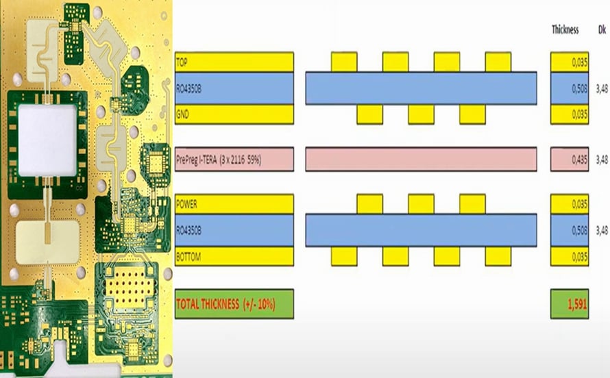
That is why layer count affects price non linearly. A four build up layer structure is not twice the cost of a two layer build up; it is considerably more, because the cumulative registration budget tightens with each cycle and yield falls unless the process is well controlled. Buyers should expect a step change in price rather than a smooth curve.
Registration and Yield
Everything in an any-layer board is small, so the tolerance stack matters. The target pad for a microvia may be fifty or sixty micrometres across, and material movement during lamination can be a comparable magnitude if the structure is not balanced. Designers help by keeping copper balanced across layers and by avoiding abrupt changes in density.
Yield then follows from process control rather than from inspection. Recentring, scaling compensation and per-panel measurements are normal practice, and a factory with a stable process will quote a realistic yield instead of an optimistic one. Comparing quotations without comparing yield expectations usually produces a misleading answer about which supplier is genuinely cheaper.
Fine Lines and Imaging
Any-layer HDI usually comes with fine line requirements, and line widths below seventy five micrometres stop being achievable with conventional subtractive etching because side etch consumes the tolerance. Modified semi-additive processing produces finer, more rectangular traces, but it requires different imaging, plating and stripping steps and more expensive equipment.
The cost is therefore tied to the design rule, not to the layer count alone. A board with relaxed line width but a four layer build up is priced differently from a board with seventy five micrometre lines and a two layer build up, and a supplier who quotes both the same way is probably not distinguishing between the processes.
Engineering and Tooling
Any-layer HDI requires more engineering before production begins. Stack up simulation, impedance modelling, drill program development, coupon design and test strategy all take time, and each new design consumes some of it. For a small order, that engineering effort is spread over fewer panels and raises the unit price considerably.
This is why the same design can cost much less per unit at higher volume. The tooling and engineering cost is fixed, the process becomes more stable as it runs, and yield improves. Buyers planning a product that will scale should ask for pricing at several quantities rather than treating a prototype quotation as indicative of production cost.
Inspection and Test Cost
Inspection in a dense board cannot rely on visual methods. Automated optical inspection struggles where traces are narrower than the camera resolution, X-ray is used to check via fill and inner layer registration, and electrical testing requires fine probe capability. Each of those stages costs money and adds cycle time.
The alternative, shipping untested boards, is not a saving. A defect that escapes into a smartphone camera module or a server board costs far more to find and correct than the inspection would have. When comparing quotations, it is worth asking explicitly which inspection stages are included and which are excluded, since this is a common source of apparent price differences.
Design Choices That Reduce Cost
Cost can be designed out without losing capability. Using any-layer construction only in the region that needs it, keeping line widths within the range the factory controls comfortably, and avoiding unnecessary stacked via structures all reduce price. So does panelisation: a design that fits efficiently on a standard panel uses material and machine time better than one that leaves large margins.
Buyers should discuss these options with the manufacturer while the design is still flexible. A supplier that can show which design rules drive cost, rather than simply quoting a number, is providing the information needed to make a considered trade off. That conversation is the practical form of design for manufacturing on a high density board.
When Any Layer Construction Is Actually Worth It
Any-layer HDI earns its premium when routing density, not component count, is the constraint. If a design can be completed on a conventional multilayer board within the available outline, the extra cost buys nothing. If the alternative is a larger product or an additional board, the calculation changes immediately.
The decision also depends on thickness. A structure with multiple build up layers can be thinner than a conventional stack with the same routing capacity, which matters in phones and wearables where millimetres decide the product. Where thickness is not a constraint, a well designed conventional board with a fine line outer layer is often the better commercial answer, and a supplier able to explain that trade is more useful than one who sells the highest specification available.
Prototype Pricing Versus Volume Pricing
Engineering, tooling and process development are largely fixed costs, so a prototype built in small quantity carries a large share of them per unit. Buyers who use that number to judge whether a design is affordable reach the wrong conclusion, and they may redesign a sound product for a cost that would have disappeared at volume.
The useful comparison is the price at the quantity the product will actually reach, together with the yield the supplier expects and the inspection stages included. Ask for both, and ask what specifically would change between the two: which steps are shared, which are repeated, and where the cost reduction comes from. Suppliers who can answer that are describing a real manufacturing plan rather than a quotation.
Working With the Fabricator Before Layout
Design rules that lower cost are easiest to apply before the layout is drawn. Whether vias may be staggered rather than stacked, how wide the fine line sections need to be, how the stack is balanced and how the panel is used all depend on the fabricator’s process, and changing them after routing is expensive.
An early conversation with the manufacturer, covering the target cost as well as the target performance, usually produces a design that is easier to build without losing capability. That is the practical value of an experienced partner on a high density project: not the ability to build anything, but the ability to say which construction delivers the required function at the lowest sustainable cost. It is a question worth asking directly when comparing suppliers of high density interconnect boards, and it is also the point at which a defined engineering process shows its worth.
Comparing Suppliers on Substance
Any-layer capability is claimed widely, so the comparison should be based on process data. Ask for the smallest stack that is in routine production, the yield achieved on comparable structures, the inspection stages included, and the change control process that applies after qualification.
Ask also what happens when a build up cycle drifts, since that is where the hidden cost lives on this class of product. A supplier with measurement data and a correction procedure will recover in days, while one without will discover the problem later, and the difference in total cost is far larger than the visible price gap between quotations. For buyers, that is where quality management translates into money.