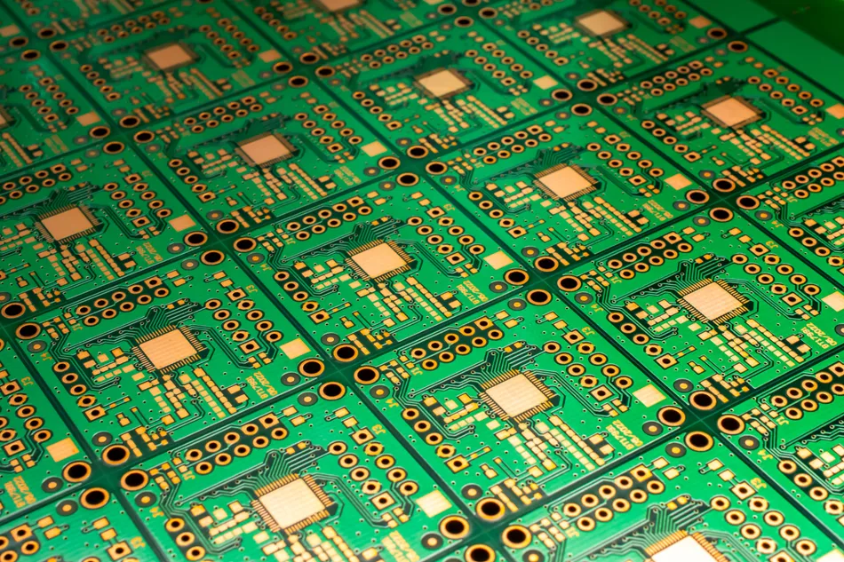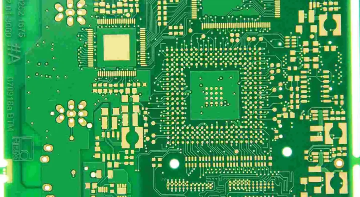
Panelization: Key Checks Before Release Panelization is the arrangement of boards into an array so that they can be processed as one unit. It decides how the boards are held during assembly, how they are separated afterwards and how much of the panel is spent on material that will be…
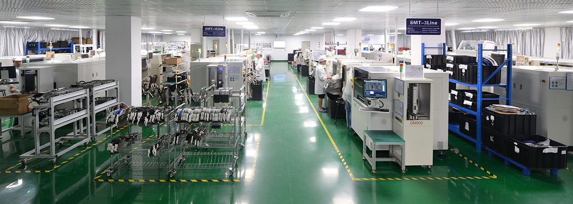
PCB Warpage After Reflow: Causes and Control Measures PCB warpage after reflow is a change in the flatness of a board caused by the heat of the soldering cycle, and it appears even on boards that were flat when they left the fabricator. The distortion is usually a few tenths…
Panel Size Selection for PCB Fabrication The panel is the manufacturing unit. It is larger than the finished board and it carries the borders, the tooling features and the array of boards that will be separated at the end. Panel size selection is a balance between the amount of material…
Laminate Storage and Handling Guide A laminate and a prepreg are reactive materials. The resin in a prepreg is partly cured and continues to advance slowly at room temperature, and both the prepreg and the finished laminate absorb moisture from the air. Laminate storage is therefore a control on two…
Component Placement Sequence Optimisation for SMT Assembly Component placement sequence is the order in which a machine places parts on a board, and it is one of the few variables in surface mount assembly that can be changed without touching the design or the process. A well ordered program reduces…
Board Thickness Selection For PCB Designs Board thickness looks like a simple choice, and in most projects it is made by default at 1.6 mm. That figure is a convention rather than a requirement, and the right thickness depends on the mechanical environment, on the connector system and on the…
Solder Mask Dam Design Between Fine Pitch Pads A solder mask dam is the narrow strip of mask that separates two adjacent pads. Its purpose is to stop molten solder from wicking from one pad to the next during reflow, and its width is one of the tightest features on…
Component Rotation Errors In SMT Assembly A component rotation error is a placement that is correct in position but wrong in orientation. The part sits neatly on its pads, so the board can pass a simple positional check, yet the polarity or the pin numbering is reversed and the assembly…
Test Point Placement For PCB Assemblies A test point is a defined place on the board where a probe can make contact for electrical test. It is the interface between the design and the test fixture, and its placement decides whether the board can be tested at all on automatic…
CTE Mismatch Design in PCB Assembly Every joint on a board is made between materials that expand at different rates. The board expands in the plane, the package expands less, the solder expands more, and the plated hole expands in a direction that the surrounding laminate does not follow. A…