Conformal Coating Process Guide A conformal coating is a thin polymer film that is applied over a populated board to keep moisture, dust and chemicals away from the circuits. The film is a few tens of microns thick, it follows the shape of every component, and it is the last…

ESD Protection Placement And Routing Rules Electrostatic discharge protection is designed as a circuit and then destroyed by its layout. A protection device that is placed a centimetre from the connector it is meant to defend will allow the transient to travel through the board, couple into neighbouring traces and…
Depanelization: Design Rules and Process Limits Depanelization is the step where the finished panel becomes individual boards. It happens after all the assembly work, which means the components, the solder joints and the board itself are all exposed to the separation force. A method that is chosen for speed can…
Desiccant and Moisture Barrier Packaging for PCB Storage Bare boards and moisture sensitive components absorb water from the air, and that water turns to steam when the part is heated. The result is delamination, blisters, cracked packages and, in the worst cases, a board that fails during reflow. Moisture barrier…
Thermal Relief Design In Copper Planes A pad that is connected directly to a large area of copper is difficult to solder, because the copper conducts heat away from the joint as fast as the iron or the oven supplies it. The usual answer is a thermal relief: a pad…
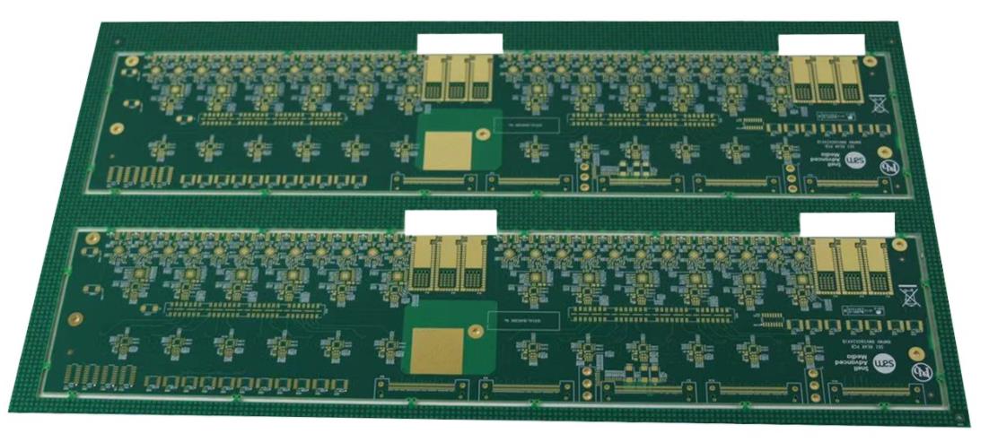
Panel Array Yield Analysis in SMT Production Yield data is generated at every station, and most of it is thrown away. A defect that is recorded only as a number tells the process engineer that something happened, while a defect recorded with its position on the panel tells them where…
PCB Fabrication Lead Time and Schedule Planning Fabrication lead time is a design variable that most projects discover too late. A stack up that requires a specialty laminate, a finish that only two shops can apply or an aspect ratio at the edge of capability all add weeks, and those…
Component Courtyard And Clearance Design Rules The land pattern defines where the solder joints are; the courtyard defines the space the part needs around them. It is the outline of the body plus the room the placement nozzle, the rework tool and the inspection equipment need to reach the part…
Selective Soldering Design Guide Selective soldering solders one joint at a time with a small fountain of molten alloy. It exists because a modern board mixes fine pitch surface mount parts with a handful of through hole connectors, and the wave process that would once have soldered those connectors would…
Wave Solder: Preparation, Placement and Process Control Wave solder is the process that solders a whole board in a few seconds by dragging it across a standing wave of molten alloy. The board design has a larger effect on the result than most engineers expect, because the solder has to…