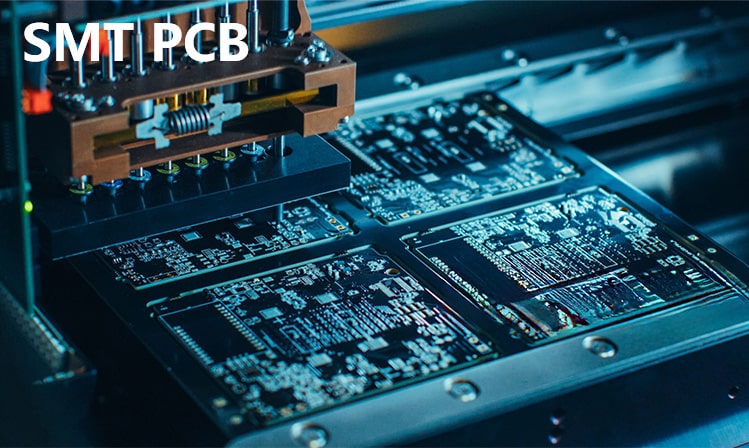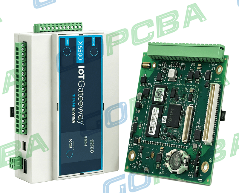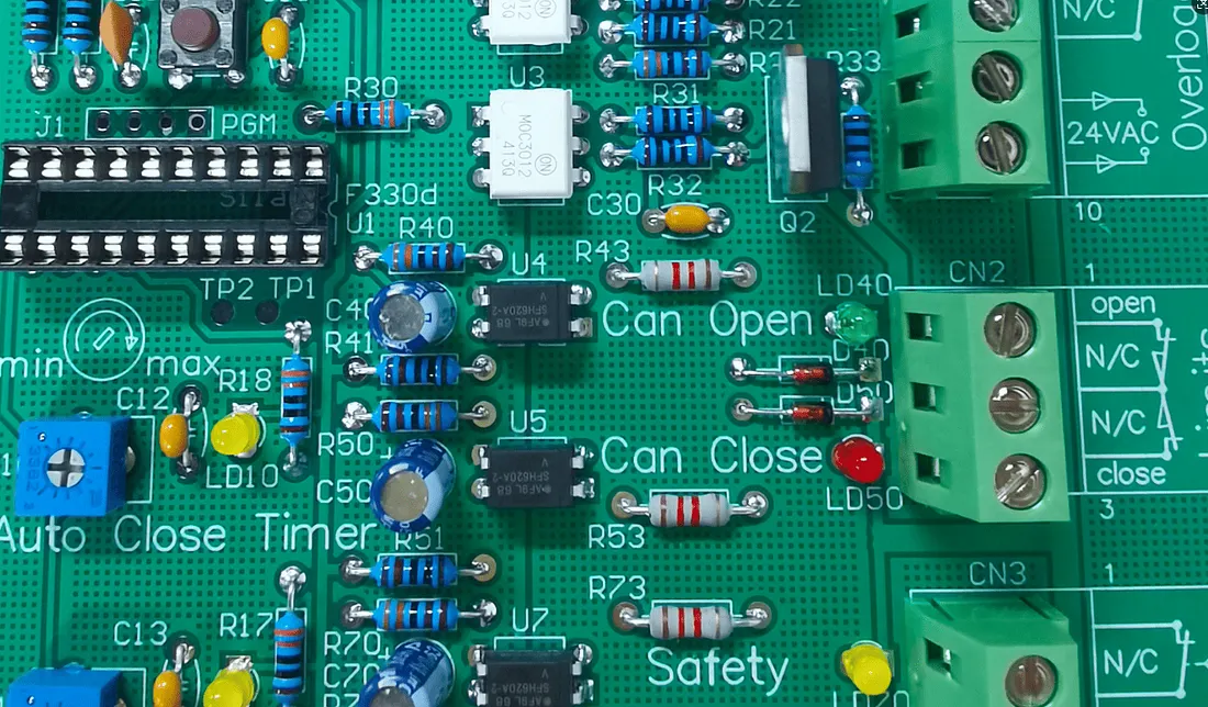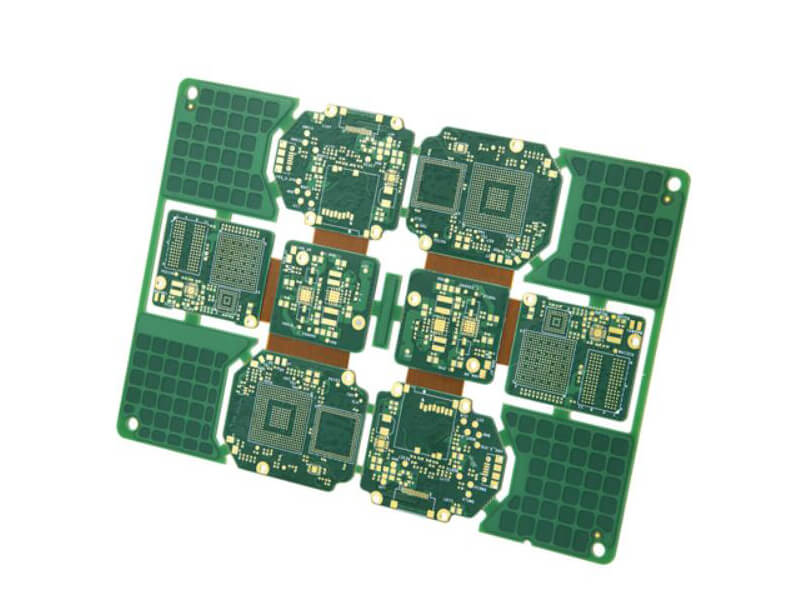
PCB Manufacturing Cost Waste: Where Money Is Lost Cost waste in board production rarely appears as one dramatic mistake. It accumulates as scrap on a panel, rework on a line, an expedited shipment and a specification that is higher than the application requires. Each item looks small in isolation, and…
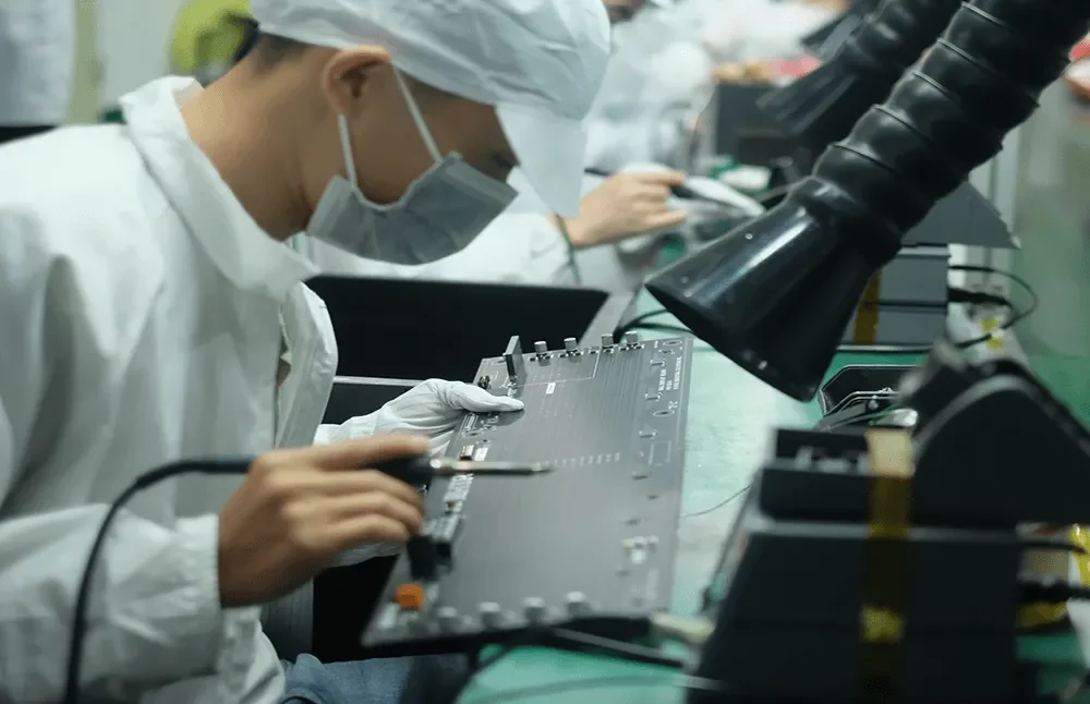
Layout Review: Fabrication Process and Quality Documentation Electrostatic discharge is a fast event with a small total energy and a very large peak current. Its effect on a product comes from two mechanisms: the current that flows through the electronics, and the field that couples into conductors before the discharge…
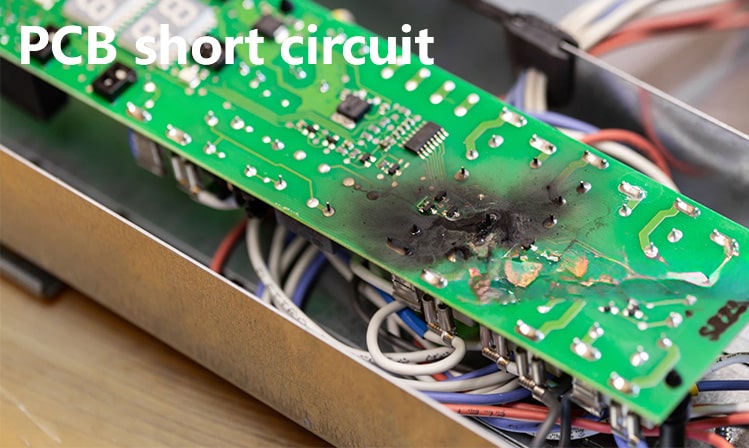
PCB Failure Modes and Environmental Testing Explained A board that passes functional test on the bench and fails six months later in the field is not unlucky. It has usually been asked to survive an environment that was never modelled during design, and the failure appears at whichever interface is…
Impedance Control From Stackup to Routing: A Working Method Impedance control is often treated as a checkbox: specify fifty ohms, tick the box, and expect the fabricator to deliver it. In practice it is a workflow in which the designer, the fabricator and the measurement instrument each play a part,…
PCB Rush Charge Explained: What Expedited Production Costs A rush charge is not an arbitrary penalty. It is the price of moving a job ahead of other jobs in a factory that is already scheduled, and it has a real cost on the production floor. Understanding what that cost is,…
When Layout Decisions Become Signal Integrity Problems A schematic can be complete, correct and fully verified, and the board built from it can still fail at the first eye measurement. The reason is that a schematic describes connectivity, not geometry. It does not say which layer a net travels on,…
100 MHz vs 1 GHz: High Speed Interfaces on the PCB An interface running at a hundred megahertz and one running at a gigahertz are separated by a factor of ten in clock rate, and by much more than that in layout difficulty. The difference is not simply that high…
Unified EDA Data Model Versus a Distributed Toolchain Hardware design has traditionally been a chain of specialised tools. Schematic capture, PCB layout, power and signal integrity simulation, and manufacturability checking each live in their own environment, connected by exported files. The workflow is familiar, but it carries a structural cost:…
PCB Panelization: Size, Spacing and Material Utilization The panel a board is built on is a shared resource, and the way a design is arranged on it decides how much of the raw material is converted into product and how much is thrown away. That arrangement is usually the shop’s…
4-Layer RF PCB Cost: Materials, Stackup and Volume Four layers is the most common stackup for RF work in the low gigahertz range, because it is the smallest construction that gives a microstrip line on the top layer, a solid reference immediately below it, and two more layers for power…