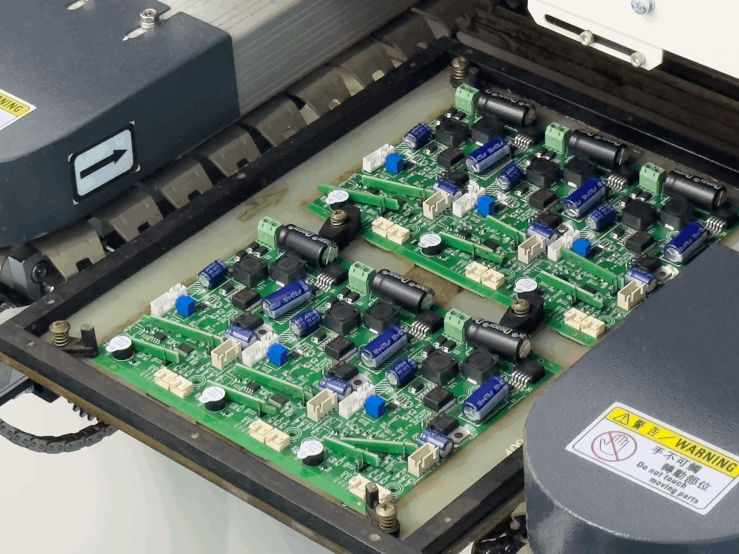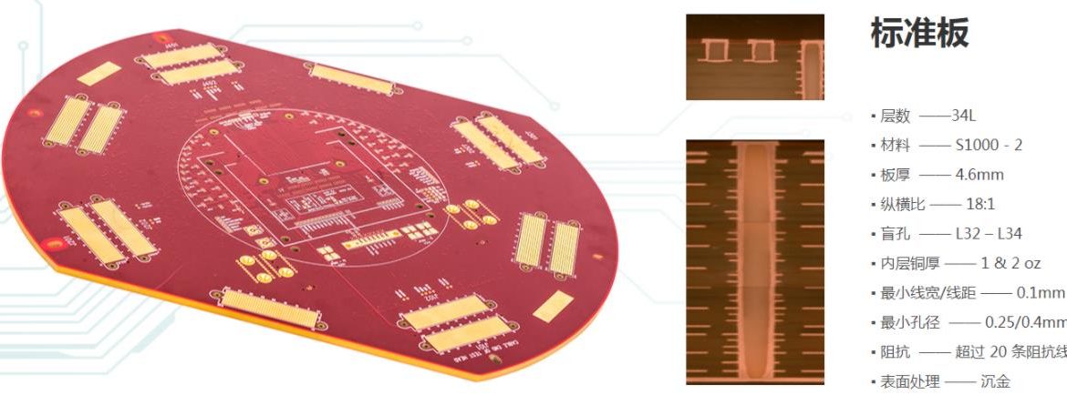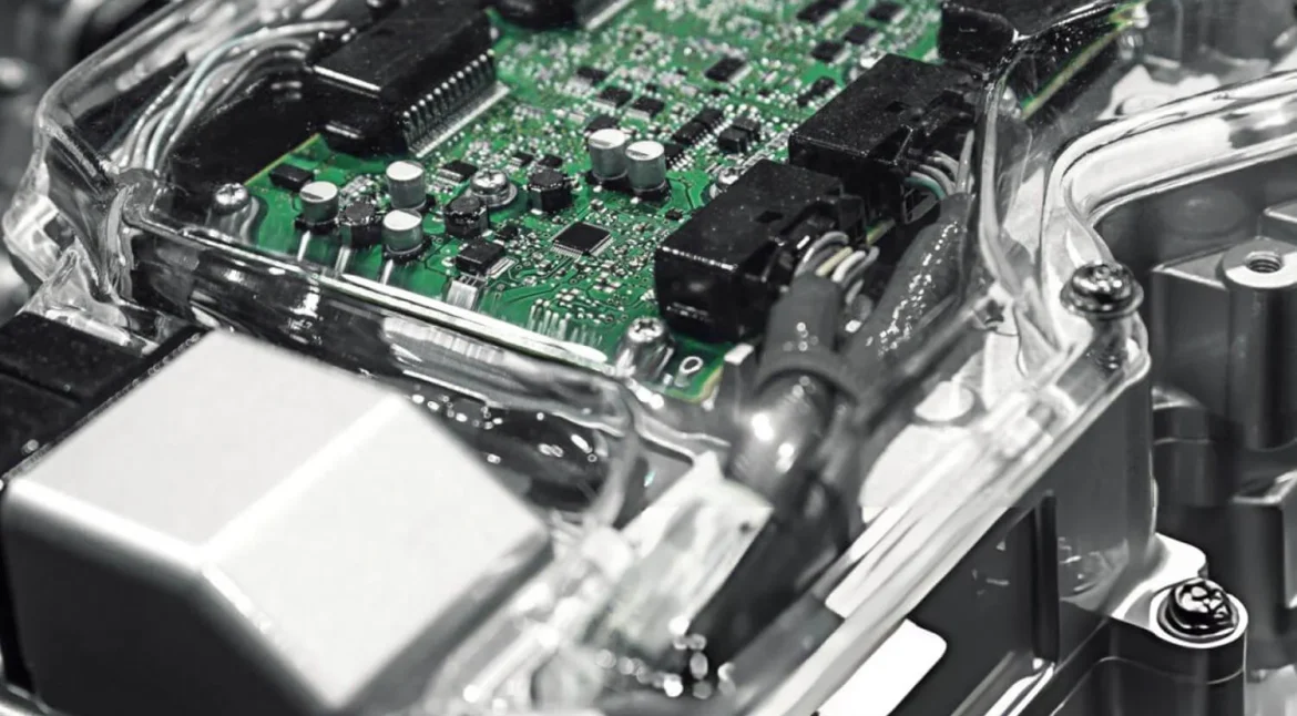
PCB Stackup Design: Principles for Multilayer Boards PCB stackup design is the least glamorous document in a hardware project and one of the most consequential. It fixes the distance between every pair of layers, decides which copper is a reference plane, and determines whether the impedance numbers in the layout…

PCB Short Circuit Prevention: Design and Assembly Practices A short circuit is the defect that wastes the most time in the assembly and bring-up phase, because it can damage parts before anyone notices it exists. Finding one after the fact is slow: the board may have hundreds of nets and…
PCB Design Workflow: Requirements, Placement and Prototyping A board design that goes smoothly is usually one where the early steps were taken in the right order. Requirements, the system design, the component choices and the schematic all constrain what the layout can achieve, and a layout that starts before those…
Alarm Panel PCB Design: Zones, Backup Power and Tamper An alarm panel PCB has to work when everything else has failed. It runs on mains with a standby battery, it monitors a set of loops that may be kilometres of wire, it drives a siren that draws several amperes, and…
Thermostat PCB Design: Sensing, Load Switching and Power A thermostat PCB has an unusually wide set of responsibilities. It measures temperature accurately, decides what the heating or cooling equipment should do, switches loads that may be mains powered, runs for years on a battery or on a few hundred microwatts…
Layout Techniques That Improve Manufacturability Manufacturability is not a separate review that happens after the layout is finished. It is a set of layout techniques that are applied while the board is being designed, and each of them either prevents a problem or moves it to a stage where it…
Through, Blind and Buried Vias: Choosing a Construction A via is a drilled hole with metal plated onto its wall, and its only job is to connect copper on one layer to copper on another. The three types differ in where the hole starts and stops, and that difference decides…
Thermal Relief and Copper Balance in PCB Design Two decisions about copper are made on almost every board and are almost never written down. The first is how a pad is connected to the plane around it, which decides how easily the joint can be soldered. The second is how…
Unintended Capacitance and Coupling in a PCB Layout Every pair of conductors on a board has capacitance between them, whether the designer intended it or not. Most of the time the value is small enough to ignore; when it is not, the effect appears as a slower edge, a coupled…
Flexible Polyimide Cost: High-Temperature Circuit Pricing Polyimide is the substrate of last resort on a cost sheet and the first choice on an environmental one. When a board has to survive 260 degrees Celsius, bend around a housing, resist solvents and keep working for a decade, the material stops being…