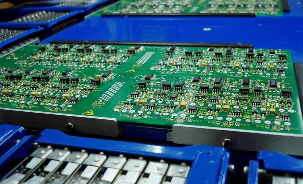
Rigid-Flex PCB Material Selection: Polyimide and Adhesives A rigid-flex PCB is only as good as the materials chosen for it, because the same assembly has to behave like a rigid board in the populated areas and like a cable in the bending areas. A material that looks adequate on a…
Migrating Design Data Between EDA Platforms Changing an EDA platform is a project rather than an installation. The copper transfers more easily than anything else; what costs the time is the data around the copper, the footprint attributes, the net names, the rules and the libraries that accumulated over years…
Copper Thickness for IoT PCB Designs: How to Choose Copper thickness is one of the few PCB parameters that touches current capacity, thermal behaviour, signal quality and price at the same time, yet it is often fixed by habit rather than by calculation. On an IoT product the decision is…
Ceramic PCB Fabrication: Alumina, AlN and DBC Technology There is a point in a design where the thermal path stops being a layout problem and becomes a material problem. A power module that has to move tens of watts through a surface the size of a postage stamp, a radio…
Automated Optical Inspection in PCB Manufacturing Inspection is the part of assembly that does not add value to the product, yet it decides whether the value produced upstream reaches the customer. Automated optical inspection has become the default way to check an assembled board because it is fast, consistent and…
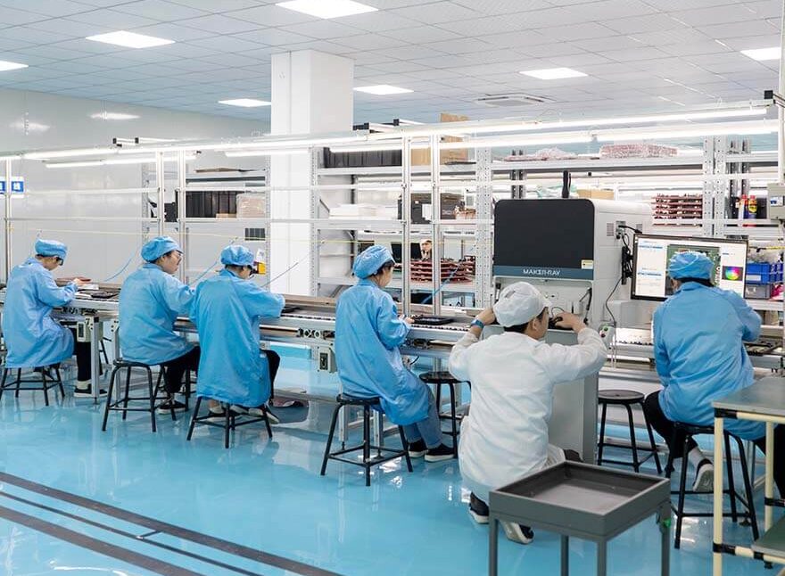
IoT Device PCB Assembly: A Step by Step Guide An IoT device usually has to do several things at once: sense something, process the data, transmit it, and survive for years on a small battery in an environment nobody controls. Each of those requirements leaves a mark on the IoT…
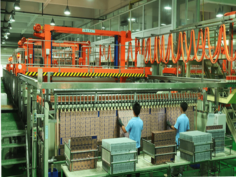
Copper Thickness and Via Plating in Multilayer PCB Fabrication A multilayer PCB is not a two layer board with more layers. The extra layers bring plated holes with a higher aspect ratio, inner layer copper that has to survive lamination, and impedance requirements that only hold if the whole process…
Parallel PCB Design Flow for Dense High Speed Boards For a long time a printed circuit board could be designed in isolation. A circuit engineer finished a schematic, handed it over, and a layout engineer routed it before passing a data package to the fabricator. Each stage worked from the…
From Design Rules to DRC: A Practical PCB Workflow A layout tool will let a designer start drawing immediately, and that is the fastest way to produce a board that has to be reworked. The work that prevents rework happens in a fixed order at the beginning: the rules are…
Signal Integrity in the PCB Design Flow Signal integrity is not a property that can be added to a layout at the end. The decisions that decide it, which layer each signal runs on, what it is referenced to, and how far it runs beside its neighbours, are all taken…