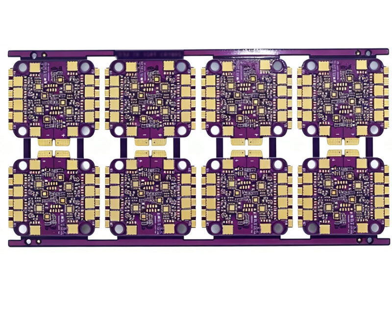
Gerber Files in PCB Manufacturing: Layers, Formats and Checks Between the design file and the finished board sits a translation step that most engineers treat as a formality. It is not. A Gerber file set is the only description of the board that the fabricator will actually use, and every…

Five Factors That Shape a PCB Manufacturing Order Two boards with identical schematics can differ threefold in price, and the reason is never the circuit. The variables that decide what a PCB manufacturing order costs and how long it takes are settled long before the order is placed, during design…
What Drives Flexible PCB Cost Flexible printed circuits are the default interconnect in products where space is tight and the harness has to bend. They are light, thin, and can be shaped to follow an enclosure, which is why they appear in phones, wearables, cameras, and instrument clusters. The cost…
PCB Gold Fingers: Plating Stack, Bevel and Wear Life PCB gold fingers are the plated strips along a board edge that slide into a socket and carry power and signals between the board and the system. They look simple, and that is why they are often specified carelessly. The plating…
PCBs With Blind and Buried Vias: Design and Applications A through hole is the simplest interconnect in a printed circuit board and, on a dense design, also the most wasteful. It occupies a footprint on every layer it passes through, whether or not it connects anything there, and a cluster…
HDI PCB vs Standard PCB: Differences and Selection Not every board has to be built the same way, and the gap between a conventional board and a high density interconnect board has widened to the point where they are almost different products. Choosing between them is not a matter of…
FFC vs FPC: Choosing a Flexible Interconnect Two flat cables look almost identical on a drawing, yet one is a set of parallel conductors laminated between plastic films and the other is a printed circuit patterned on a flexible substrate. The difference decides cost, tooling, bend behaviour and how much…
4-Layer PCB Design: Stackup, Placement and Routing Steps Four layers is the point where a board stops behaving like a flat piece of copper foil and starts behaving like a transmission system. It is also the layer count where most products find their best balance of cost, routing freedom and…
Why Multilayer PCB Design Beats a Double-Sided Board Adding layers to a board is the most expensive single decision in most projects, and also one of the most misunderstood. Engineers often assume that more layers automatically mean better performance, while cost engineers assume that fewer layers always means a cheaper…
PCB Lamination Process Step by Step Lamination is the step that turns a stack of separate layers into a single board. It is the longest single operation in multilayer fabrication, and it is the point at which the electrical and the mechanical properties of the finished board are decided. Getting…