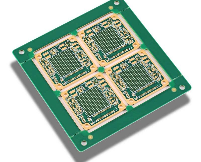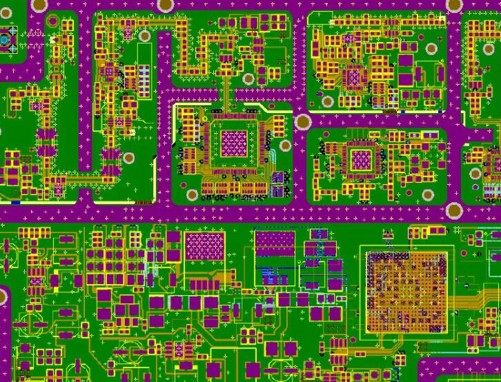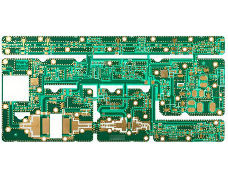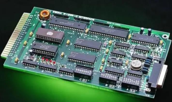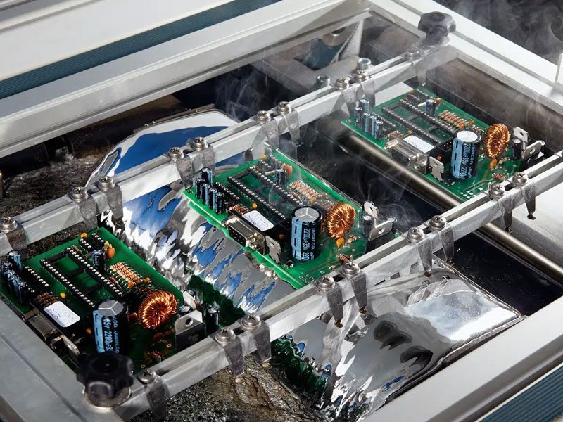
Multilayer Board Faults: Shorts, Opens and Bad Vias A multilayer board that fails is usually failing for a reason that was designed in months earlier. Shorts, opens and intermittently connected vias rarely come from one bad process step; they come from clearance that was too tight, a via barrel with…
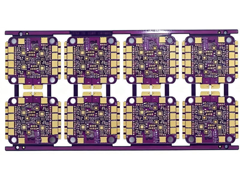
Double-Sided PCB: Definition, Structure and Applications A double-sided pcb occupies an unglamorous middle position in the market, and that is exactly why it ships in such volume. It costs far less than a multilayer stackup and offers far more routing freedom than a single-sided board, so it lands in the…
PCB Inspection Steps: How Boards Are Checked Before Shipping A finished board looks identical whether it was built carefully or merely plausibly. What separates the two is the inspection sequence behind it: a series of checks, each performed at the point where a defect is still cheap to correct. Understanding…
PCB Plating Types and Thickness: How to Choose a Finish Surface finish is one of the last decisions a designer makes and one of the first that assembly engineers ask about. It determines how well solder wets the pad, how long the board survives on a shelf, and whether a…
PCB Routing Rules: Current Path, Return Path, and Crosstalk Routing quality decides whether an electronic product performs, survives, and ships on schedule. The same schematic can produce a quiet board or one that resets when a motor starts, and the difference is almost always in the routing. The rules below…
PCB Routing Guide: Trace Width, Spacing and Return Paths Pcb routing is the stage where a schematic becomes physical copper, and it is where most of the electrical performance of a board is actually decided. Placement sets the possible solutions and the stackup sets the impedance, but the path each…
The BOM in PCBA: Bill of Materials Control That Prevents Delays Every assembly quotation starts with the same request, and it is not the Gerber files. The assembler needs a bill of materials, because that single document defines what has to be bought, how the line has to be set…
PCB Level Shielding: Board Shields, Cans and Faraday Cages Enclosure shielding is the first line of defence against radiated emissions, and on modern products it is increasingly compromised. Ventilation openings, display windows, cable penetrations and connector cut-outs all break the shield, and the degradation is not gradual: a single large…
High-Speed PCB Via Design: Parasitics and Sizing On a fast board, the via is usually the weakest electrical element in the interconnect. It is short, it is cheap, and it is invisible on the schematic, yet it adds capacitance to the trace, inductance to the return path, and a stub…
HDI PCB Technology and Microvia Design Rules A high-density interconnect board is not simply a multilayer board with more layers. It is a board whose interconnect is dense enough that ordinary through-hole vias can no longer serve every connection, so the design moves to smaller holes, finer features and vias…