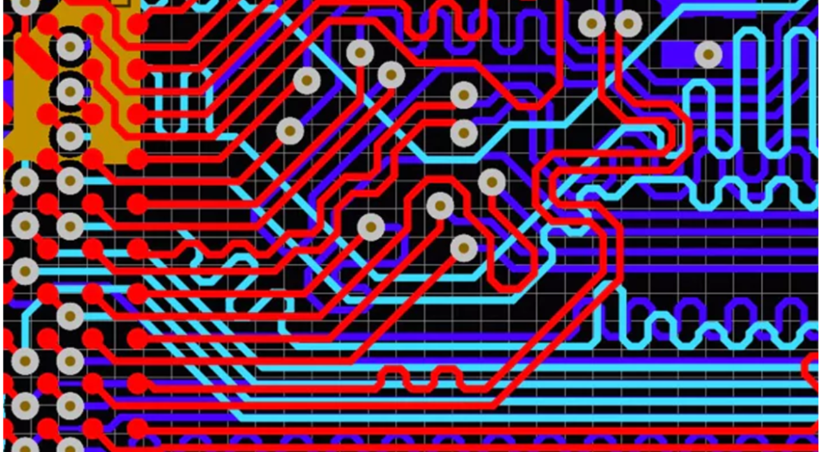
PCB Design Layers Explained: Signal, Plane, Mask, and Mechanical Modern layout software presents the design as a stack of named layers, and new engineers often find the number of them overwhelming. Each layer has a specific role, and each one produces a different output file or a different instruction to…
Metal Core PCB Design and DFM: Stackup, Vias and Grounding Metal core boards are rare in consumer products and everywhere in lighting, power conversion, industrial drives and aerospace equipment. The reason is simple: a high power stage produces heat that has to leave the package quickly, and a glass reinforced…
PCB Etching Quality: Undercut, Etch Factor and Defects PCB etching quality is decided long before the panel reaches the etcher, even though this is the step that finally reveals the circuit pattern. In a pattern plating process, a resist layer is plated onto the copper that must remain and the…
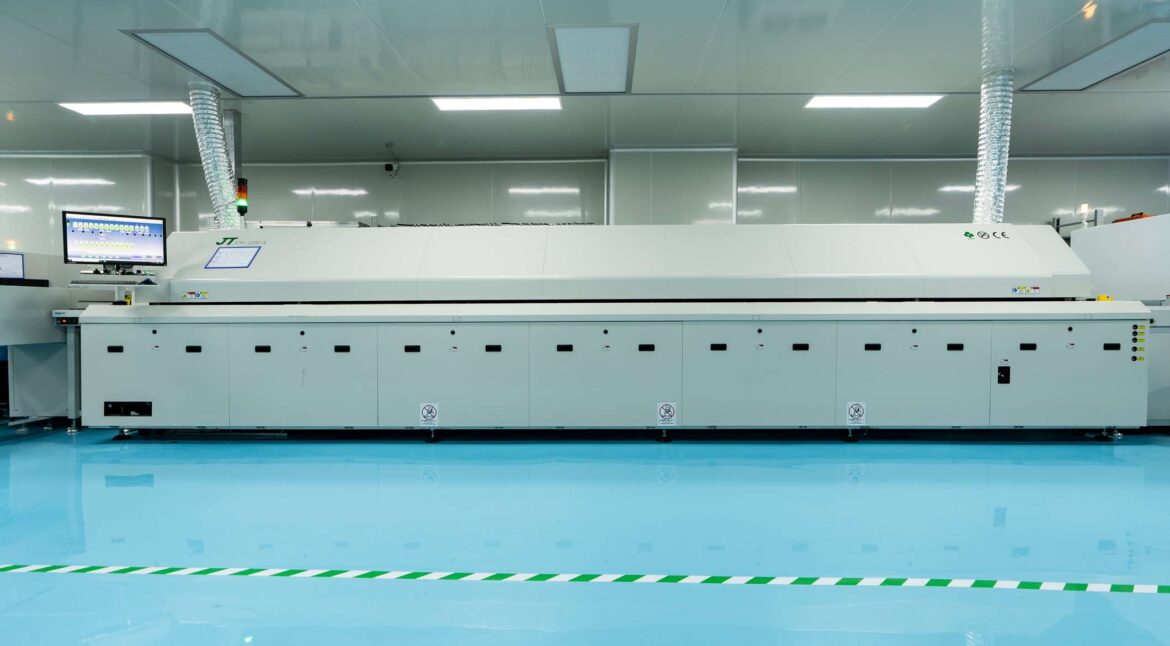
Solder Bead Defects in SMT Assembly: Causes and Fixes Solder beads are the small spheres of alloy that appear on an assembly surface after reflow, sitting beside a joint instead of being part of it. A single bead of 0.3 mm looks harmless on the bench, but once it breaks…
PCBA Soldering Requirements: Board Size, Fiducials, and Flatness A board can be electrically flawless and still be rejected by the assembly house, because the soldering process imposes its own requirements on the physical design. Panel dimensions, edge conditions, flatness, fiducials, and pad geometry all have to be compatible with the…
Reference Designators on a PCB: Prefix Letters and Numbering Rules Every component on a board carries a short code printed next to it, and that code is the language the assembly line, the test engineer, and the repair technician all rely on. A reference designator is the combination of a…
IC Substitution: Rules for a Safe Second Source Component shortages have made second sourcing a normal part of hardware development rather than an exception. When the specified device is unavailable, the question becomes whether a similar part from another manufacturer can be used without changing the board. IC substitution is…
Laser Processing in PCB Manufacturing: Cutting, Drilling, Depaneling Laser processing entered PCB manufacturing as a way to solve problems that mechanical tools handle poorly: very small holes, shapes that a router cannot follow, and panels that cannot tolerate mechanical stress. It is now used across drilling, cutting, depaneling and direct…
SDRAM Radiation: Layout Rules for External Memory External memory is one of the most common sources of radiated emissions on a microcontroller board, and it is one of the most fixable. A parallel SDRAM bus runs at a high clock rate with fast edges, and its traces carry the same…
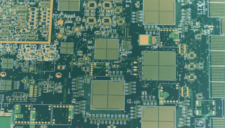
High Precision PCB Manufacturing: Fine Lines and Microvias Density on a printed circuit board is increased by making conductors narrower and holes smaller, and both changes push the process into a region where tolerance, not capability, becomes the limiting factor. A board shop that can hold a 0.20 mm line…