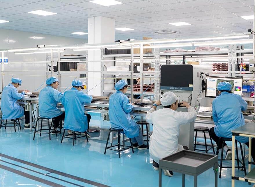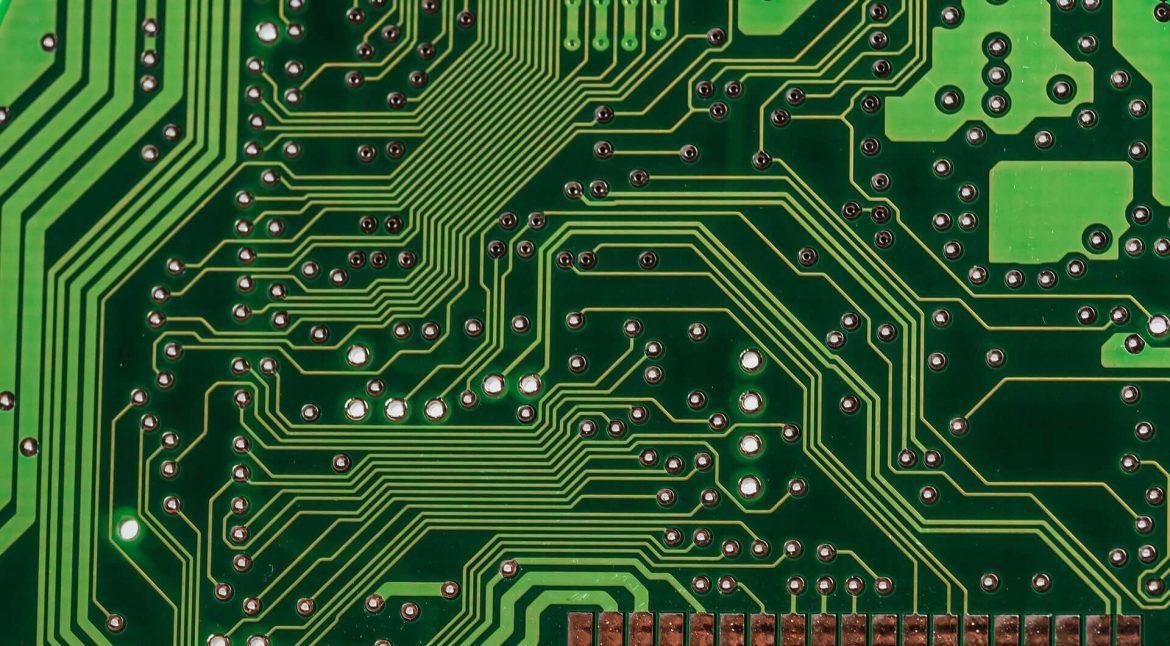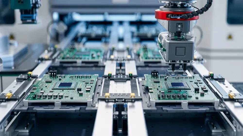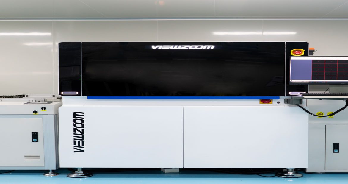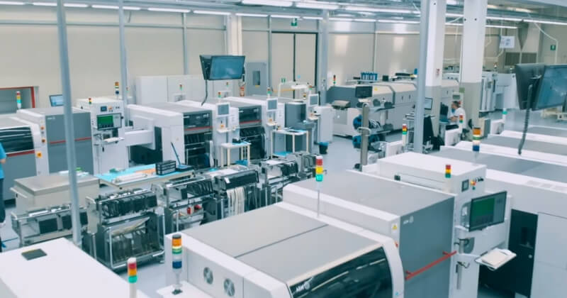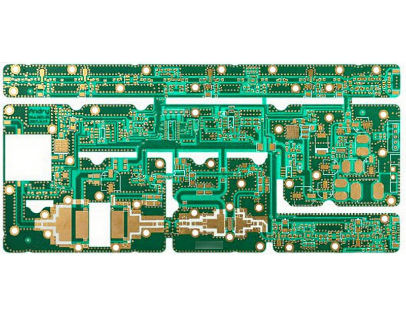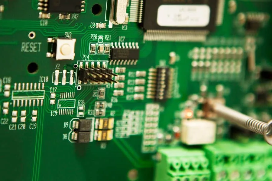
PCB Production Process: From Cutting and Drilling to Final Test A printed circuit board starts as a sheet of copper clad laminate and ends as a tested substrate with copper features measured in tens of microns. The PCB production process between those two points is a sequence of additive and…

Why 32 Layer Board Prototypes Cost More A high layer count board is expensive for reasons that go well beyond the price of the material. Each added layer multiplies the number of interfaces that must be bonded and aligned, lengthens every process step and reduces the proportion of boards that…
TVS Diode Selection and Placement for ESD Protection Every board that connects to the outside world needs a defined answer to the question of what happens when a discharge arrives. A transient voltage suppression diode is the most common answer, because it responds in fractions of a nanosecond, absorbs a…
Surface Tension and Viscosity in Solder Wetting Solder does not flow because it is pushed; it flows because the forces around it are balanced in its favour. Surface tension acts to minimise the free surface of the liquid, and viscosity resists the movement of the liquid itself. Both work against…
EMC Immunity Testing: Radiated Field Susceptibility Immunity is the other half of electromagnetic compatibility, and it is usually the harder half to test. Emissions can be measured without touching the product; immunity requires the product to be operating normally while a disturbance is applied, and the failure may be a…
PCB Layout for Soldering: Design Choices That Decide Yield Most soldering defects are not created at the soldering station. They are created by a pad that is too wide, a via placed in the middle of a pad, a fiducial that the vision system cannot see, or a component rotated…
PCB Size and Shape Requirements: Defining the Board Outline A printed circuit board has to fit the application it was designed for, and the application dictates the size and the shape. That sounds obvious, yet the outline is often the last thing to be finalised and the first thing to…
Aluminum PCB Advantages and Applications Most boards are built on a laminate chosen for its electrical properties, and the heat has to be carried away by copper and by air. An aluminum PCB reverses that priority. The substrate is a metal plate, and the board is designed around getting heat…
Depth-Controlled Milling on PCB Panels: Holding Z Tolerance Some boards cannot be profiled with a through-cut. Where a recess has to be milled to a controlled depth, or where a cavity must stop a fraction of a millimetre above an inner layer, the routing depth becomes a process parameter in…
Mobile Phone PCB Layout: Layer Plan and Routing Order A handset main board packs a radio, a baseband processor, memory, power conversion and a display interface into a space smaller than a business card. The mobile phone PCB layout that makes this possible is not a single clever trick but…