Aerospace PCB Assembly: Designing for the Space Environment Aerospace electronics are not simply rugged versions of industrial hardware. The environment is different in kind: radiation that can corrupt logic, temperature swings of hundreds of degrees, vibration and shock during launch, and a service life during which no repair is possible.…
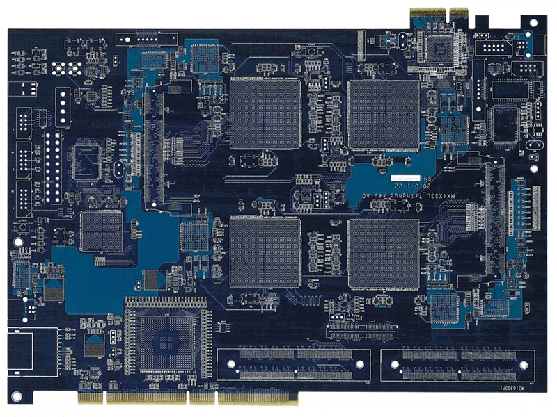
PCB Production Process Complexity: Why Board Builds Get Hard Printed circuit board manufacturing is unusual among production processes in that it combines mechanical machining, photochemistry, electrochemistry, heat and pressure, and computer-aided data preparation in a single flow. Each step is only as good as the one before it, the work…
Aluminum PCB Substrate: Thermal Performance and Application Scope An aluminum PCB substrate replaces the usual glass-reinforced epoxy with a metal base, typically a low-alloy aluminum sheet with a thin insulating dielectric layer bonded to it and the copper circuit formed on top. The construction exists for one reason: to move…
PCB Layout Constraints: Six Checks Before Placement A board that works electrically can still be a bad board. It may not fit the enclosure, it may not panelise, it may run hotter than the thermal design assumed, or it may pass an EMC test on the bench and fail in…
Ground Pour Under Crystal: Why the Imaging Plane Matters The oscillator is the quietest part of a digital board and the easiest to turn into a radiator. Its output switches at a fixed frequency with fast edges, and the return current for those edges follows the reference plane beneath the…
PCB Layout Basics: Footprints, Netlists, Ratlines, and Copper Pour Most layout questions that stop a project are not about signal integrity. They are about the design database: which footprint belongs to which part, what a ratline actually means, why a netlist can differ from the schematic, and when copper pour…
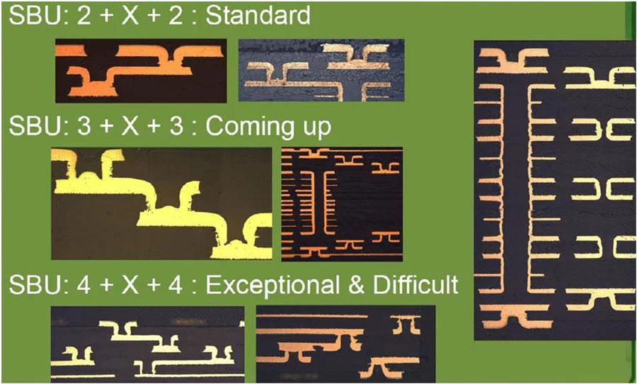
Additive PCB Process Routing Rules for Fine-Pitch BGA Fan-Out Package pitches have fallen from 1.0 mm to 0.8 mm, then to 0.4 mm, and the escape routing problem has become the dominant constraint in the layout of large devices. At those pitches a conventional etch process cannot produce conductors fine…
Copper Island Keep or Remove: Dead Copper and the Antenna Effect Almost every layout ends up with copper that is connected to nothing: a patch left behind after a plane is cleared, a sliver cut off by a keep-out, or a remnant of a pour that no net reaches. Manufacturers…
Key Production Processes for High Layer Count PCBs Average layer count has become one of the standard measures of a board shop’s technical level, and for good reason. High layer count PCBs are not simply thicker versions of a normal multilayer board. It combines more layers with thinner dielectric, denser…
Surface Mount Technology Advantages in Wireless Charging Board Production Surface mount technology is now the default method of building electronic hardware, and it is worth understanding why, because the reasons are not only about speed. Removing the drilled hole from the process changed the economics of assembly, the electrical behaviour…