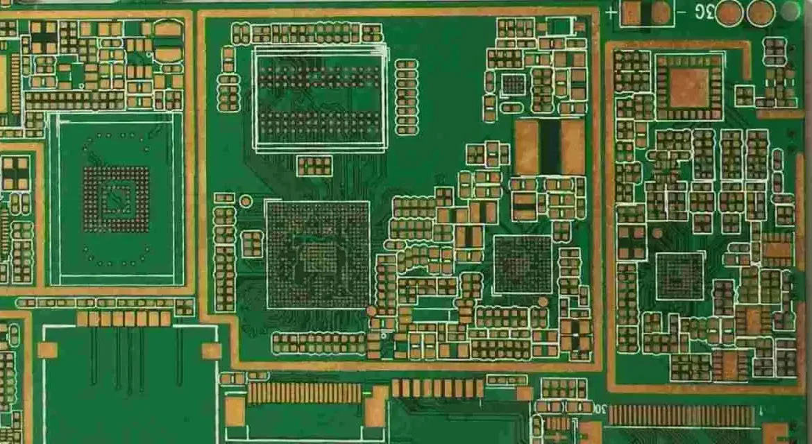
Electronic PCB Assembly: Design Rules That Improve Assembly Yield Assembly is the last chance to influence yield, and by the time a bare board reaches the placement machine most of the cost has already been committed. The design decisions that determine whether the assembly runs smoothly are made months earlier:…

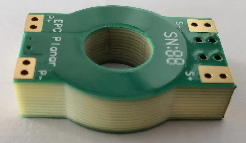
PCB Stackup Design: Layers, Reference Planes, and Return Paths Stackup design is where the electrical requirements of a board are translated into physical layers, and it is usually the last decision to be revisited and the first one to cause problems. How many signal layers are needed, how many planes,…
Vacuum Etching in PCB Fabrication: Eliminating the Puddle Effect Etching is the step where the copper pattern finally becomes real, and it is also where fine-line capability is won or lost. The difficulty is not removing copper but removing it uniformly, because the etchant that has already reacted with the…
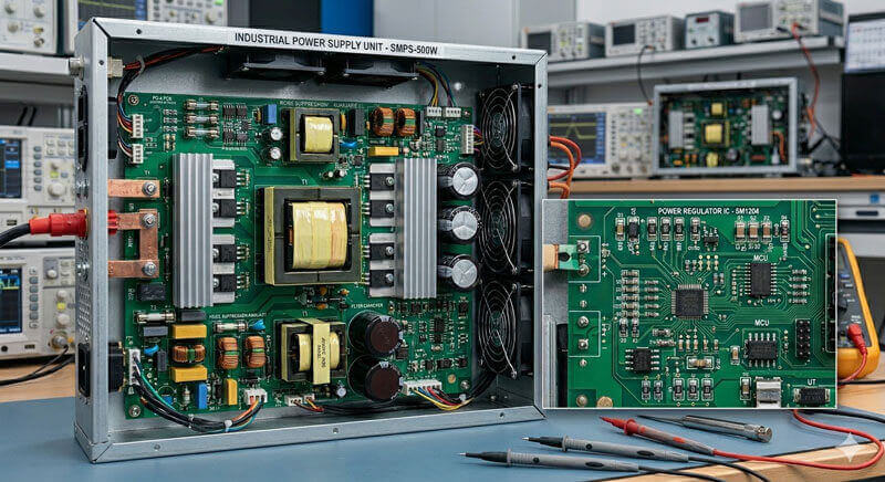
Power Board SMT Assembly: Process Requirements and Spacing Rules Power boards are not ordinary surface-mount assemblies. They carry large devices that dissipate real heat, they often use thicker copper to handle the current, and they frequently combine a dense surface-mount section with heavy through-hole parts. Those characteristics change the requirements…
PCBA Assembly Process Selection: SMT, DIP, and Mixed Flows Once a board is designed, the next decision is how it will be assembled, and the options are not interchangeable. The mix of surface-mount and through-hole content, the number of sides that carry components, and the thermal sensitivity of the parts…
PCB Reliability: Characteristics of a High-Quality Board Two boards can look identical and behave completely differently over a five-year service life. The difference is rarely visible on the surface, but it is decided by a set of measurable characteristics that a fabricator either controls or does not. PCB reliability comes…
Blind and Buried Vias in HDI PCB Manufacturing When routing density rises far enough, a through hole becomes an unaffordable use of the board. It occupies a landing pad on every layer, blocks the routing channels around it on every layer, and prevents the layers above and below from being…
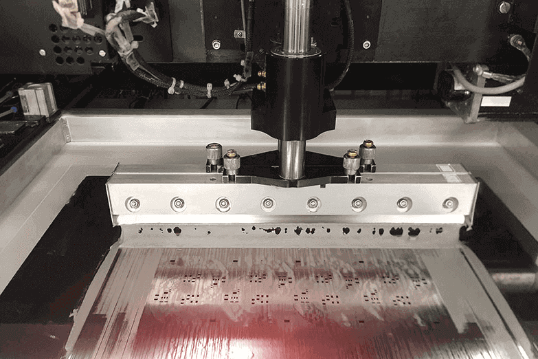
SMT Assembly Data Package: Gerber, BOM and Placement A surface-mount build starts long before the first panel is printed, and it starts with data. When the assembly package is incomplete, the factory stops, asks questions and waits, and the lost time lands directly on the delivery date. A complete SMT…
PCB Electrical Clearance and Spacing Requirements Explained Spacing is the part of a layout that nobody notices until the board fails. A trace that runs 4 mil from its neighbour is a reliability experiment, not a design; a pad that sits 0.1 mm from the board edge is a short…
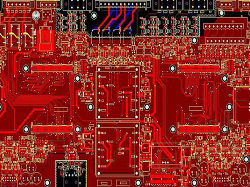
Five Key Points of PCB Board Design Most of what determines whether a board is quiet, manufacturable and easy to build comes down to five decisions that are made before detailed routing begins. None of them is complicated, and all of them are easier to get right at the start…