Ground Routing and Power Trace Planning Routing begins with a decision that is easy to postpone and expensive to revisit: where the ground and the power go. Signal traces are what designers picture when they think about routing, but the ground and power distribution network is what determines whether the…
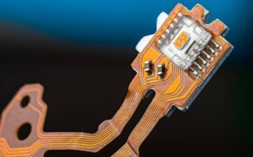
PCB Slot Design Rules and Edge Routing A slot is a cut in the board that is not a hole and not the outline. It may separate a high-voltage section from a low-voltage one, allow air to move across a hot component, provide a mounting feature, or define a breakaway…
Serpentine Routing: Length Matching Done Correctly When two signals leave a source at the same instant and must arrive at the same instant, their traces have to be the same electrical length. Real boards rarely allow that naturally, so the designer adds length to the shorter path. The usual way…
Mixed Signal PCB Design Guidelines Boards that contain both analog and digital circuits are the most common source of difficult layout problems, because the two halves of the design want opposite things. Analog circuitry measures small continuous signals and needs a quiet, stable reference. Digital circuitry switches state abruptly, draws…
Trace Width and Current: Calculating the Right Copper Sizing a trace for current is one of the few layout decisions with a closed-form answer, and it is also one of the most frequently skipped. A trace that is too narrow will heat up, increase its resistance, heat up further, and…
Blind Via and Buried Via Stack Selection A through via is the simplest way to connect two layers, and for most designs it is still the right answer. Choosing between the structures is really a question of how many lamination cycles the complete via stack requires. It is drilled once,…
DC-DC Converter Layout and Routing Guidelines A switching regulator converts voltage efficiently because it never operates the pass device in its linear region. The cost of that efficiency is a node that switches between the input rail and ground at hundreds of kilohertz to several megahertz, and every trace connected…
STM32 Core Board PCB Design: Rules and Layer Planning A microcontroller core board looks simple: one large device, a handful of passives and a connector that breaks out the pins. In practice it is one of the harder boards to lay out well, because the processor is fast, the power…
Potting Compounds and Dispensing Adhesives on PCBs Not every board lives in a dry, temperature-controlled cabinet. Products used outdoors, in vehicles, in kitchens or on factory floors are exposed to moisture, dust, salt and vibration, and the electronics inside them have to keep working for years. Potting and dispensing are…
The 3W Rule: Trace Spacing for Crosstalk Control Crosstalk is the least visible of the signal integrity problems and the one that designers most often try to solve with a rule of thumb. The 3W rule is the best known of those rules: keep the centre-to-centre spacing between two traces…