Land Pattern Errors: Why Pads Spaced Too Far Apart Fail in Reflow Most footprint errors are obvious once they are pointed out: a pad that is too short, a wrong pin numbering, a missing thermal pad. The one that causes the most trouble in production is more subtle. It is…
PCB Short Circuit: Finding and Preventing the Ones That Escape A short circuit on a finished board is expensive because it usually appears after the material and the assembly time have been spent. The causes are few and well understood, which means most of them can be designed out and…
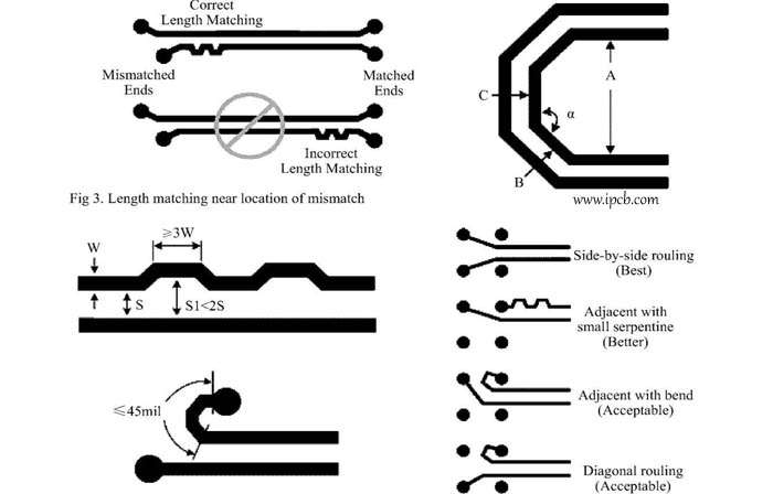
Layer Change or Detour: Choosing Between a Via and a Bend The question comes up on almost every high speed layout: is it better to change layer through a via, or to stay on the same layer and route around the obstacle? The two options trade one discontinuity for another,…
High Frequency PCB Routing: Fewer Vias, Shorter Paths, Less Coupling High frequency PCB routing follows from a small number of physical facts. A trace radiates in proportion to its length, a via adds capacitance and a discontinuity, a corner reflects, and two parallel traces exchange energy. Every rule below is…
Power Plane Design: Splits, Necking and Decoupling on the Board A power plane is often treated as the easy layer: pour copper on the net and move on. In practice the plane is the return path for every signal above and below it, and it is the distribution network that…
PCB Design Reuse: Snippets, Device Sheets and Multichannel Blocks Most boards contain a circuit that has already been designed somewhere else. A power supply stage, a converter interface, a memory block, a connector section: these are the parts of a design that are repeated across projects, and the way a…
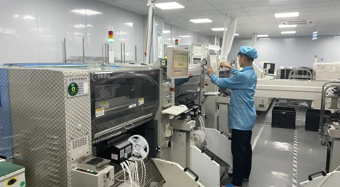
BGA Assembly: Placement, Reflow and How the Joints Are Inspected A ball grid array is a package whose connections are underneath the body rather than around the edge. That single change of geometry is what makes the package attractive, because it allows hundreds of connections in a small area, and…
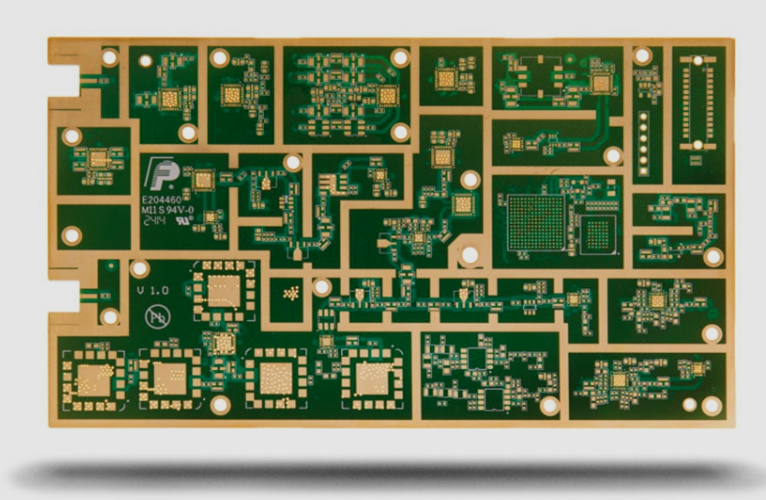
RF PCB Design: Impedance Control and Isolation on the Board Radio frequency circuits are designed in two places at once. The schematic sets the topology, the matching and the gain, and the layout determines the impedance of every connection between those components. A perfect schematic on a board that ignores…
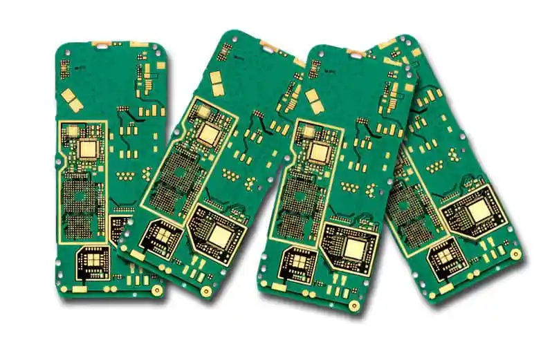
PCB Design Mistakes: The Errors That Reach Production Most of the errors that stop a board from being built are not electrical. They are documentation and geometry mistakes that pass a design rule check because no rule covers them, and they surface when the fabrication data is processed or when…
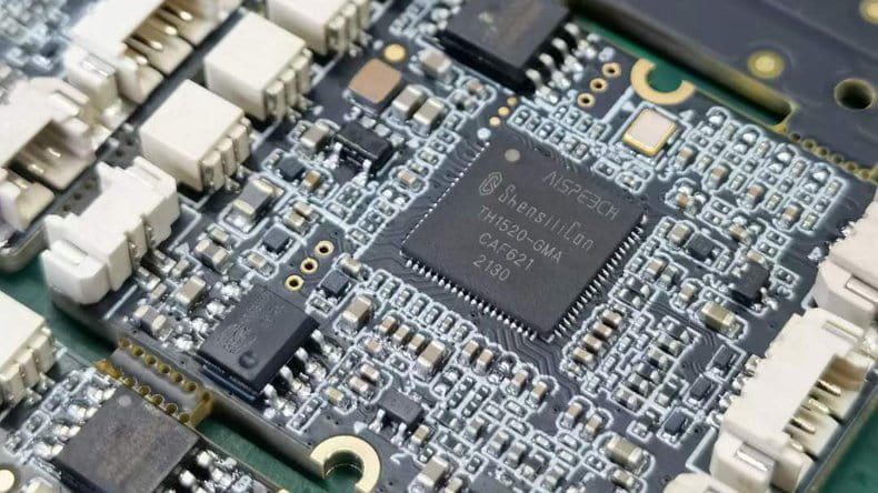
PCB Quality Inspection: What You Can Judge Without a Microscope Not every quality question requires a laboratory. When a batch of bare boards arrives, several of the characteristics that separate a controlled process from an approximate one are visible to the naked eye, or with modest magnification. None of them…