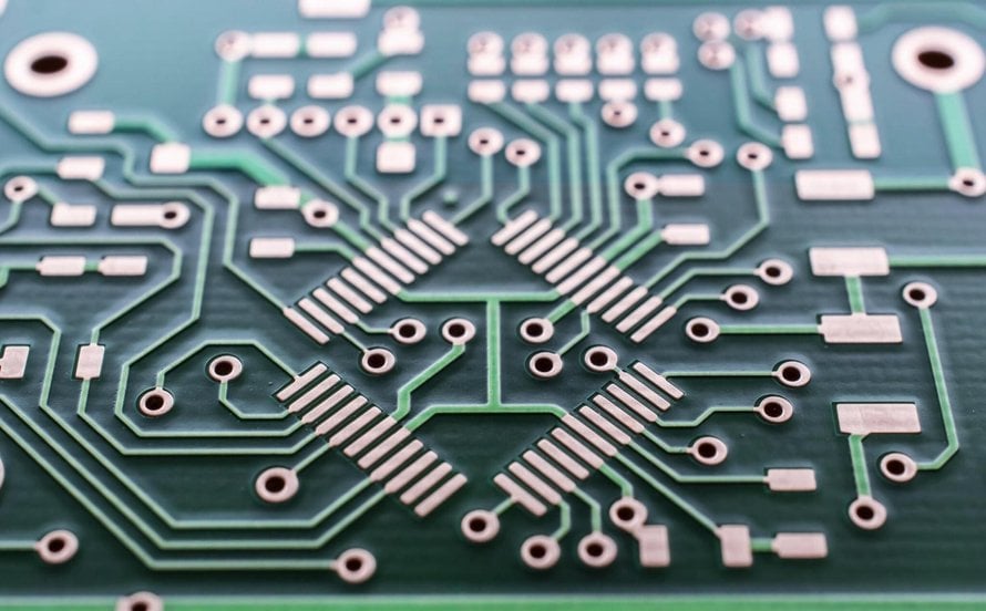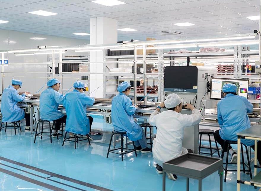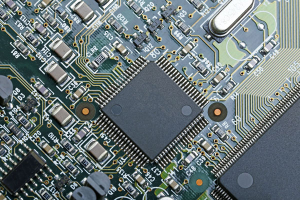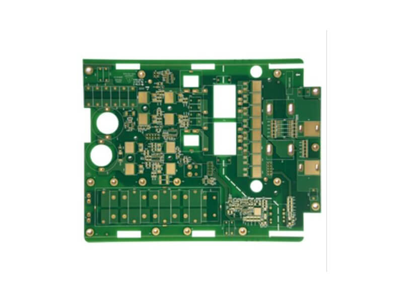
HDI Blind and Buried Via Process: Laser Drilling to Plating High-density interconnect boards fit more routing into less area, and the HDI blind and buried via process is what makes that density practical. A blind via connects an outer layer to an inner layer without passing through the whole board;…
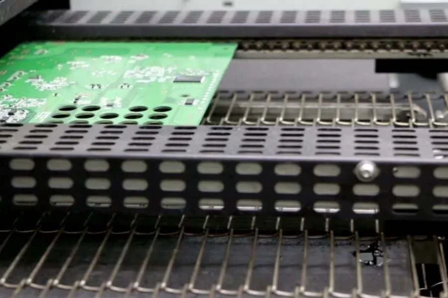
PCB Medical Device Process Validation: Proving the Process Electronics manufacturing has become a discipline of small details. Solder paste volumes, placement accuracy, temperature profiles and inspection limits all add up to the final result. This guide looks at PCB medical device process validation from the perspective of a PCBA factory…
PCB AS9100 Requirements for Aerospace: The Aerospace Rules Buyers and engineers often focus on the finished product and forget the production line behind it. In practice, most field failures can be traced back to process decisions made during assembly. Understanding PCB AS9100 requirements for aerospace gives you a practical advantage…
PCB IATF Requirements for Automotive: The Automotive Rules Electronics manufacturing has become a discipline of small details. Solder paste volumes, placement accuracy, temperature profiles and inspection limits all add up to the final result. This guide looks at PCB IATF requirements for automotive from the perspective of a PCBA factory…
PCB ISO 9001 Audit Evidence: Showing the System Works Buyers and engineers often focus on the finished product and forget the production line behind it. In practice, most field failures can be traced back to process decisions made during assembly. Understanding PCB ISO 9001 audit evidence gives you a practical…
PCB Design and Prototyping: Optimizing the Development Flow Prototyping is where a design stops being a drawing and starts producing data. The schedule risk in a hardware project is rarely in the schematic; it sits in the two or three weeks between finishing the layout and holding a working board,…
PCB Circuit Board Design Steps: Requirements to Production Files A circuit board that works on the first prototype is not the product of a single clever decision. It is the result of a sequence of steps, each of which narrows the options available to the next. Skipping a step does…
PCB Third Party Certification Audit: The Outside Inspector Modern electronics depend on boards that are assembled correctly the first time. Every product – a phone, a charger, a medical instrument or an industrial controller – relies on thousands of solder joints that must conduct current for years. This article explains…
PCB Outline Design: Outline Layer, Panelization and Tolerances Most layout reviews spend their time on impedance and length matching and treat the board edge as a formality. The edge is what the fabricator machines first, what the assembler clamps, and what decides whether a thin product survives its own reflow…
AI Server PCB Design: HDI, High-Speed Buses and Power The boards inside a training cluster are no longer oversized server motherboards. They are high-layer-count interconnect carriers whose job is to move hundreds of gigabytes per second between accelerators and to deliver several hundred watts to each of them without sagging.…