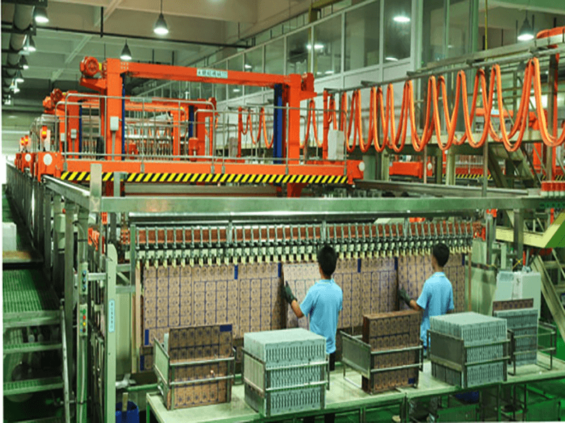
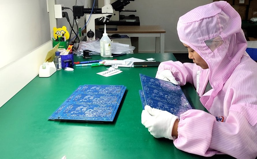
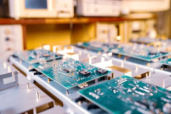
PCB Board Support Pin Wear: Holding the Board Steady Buyers and engineers often focus on the finished product and forget the production line behind it. In practice, most field failures can be traced back to process decisions made during assembly. Understanding PCB board support pin wear gives you a practical…
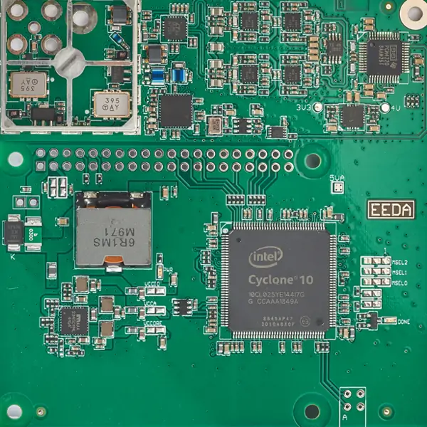
PCB Depaneling Blade Wear: When the Cut Starts to Tear Buyers and engineers often focus on the finished product and forget the production line behind it. In practice, most field failures can be traced back to process decisions made during assembly. Understanding PCB depaneling blade wear gives you a practical…
Coin Insertion PCB: Embedded Copper for Heat and Current Why a Board Needs Metal Inside It Power density is the constraint that shapes modern boards. A MOSFET, an insulated gate bipolar transistor module or a power management IC can dissipate tens of watts from a package a few millimetres on…
PCB Component Overhang at Panel Edge: Parts That Cross the Line Buyers and engineers often focus on the finished product and forget the production line behind it. In practice, most field failures can be traced back to process decisions made during assembly. Understanding PCB component overhang at panel edge gives…
PCB Array Spacing Between Boards: Room to Separate Them Electronics manufacturing has become a discipline of small details. Solder paste volumes, placement accuracy, temperature profiles and inspection limits all add up to the final result. This guide looks at PCB array spacing between boards from the perspective of a PCBA…
PCB Bad Mark for Panel: Marking a Board That Failed Modern electronics depend on boards that are assembled correctly the first time. Every product – a phone, a charger, a medical instrument or an industrial controller – relies on thousands of solder joints that must conduct current for years. This…
PCB Panel Fiducial Layout: Marks for the Whole Panel Buyers and engineers often focus on the finished product and forget the production line behind it. In practice, most field failures can be traced back to process decisions made during assembly. Understanding PCB panel fiducial layout gives you a practical advantage…
High Frequency RF PCB: Materials, Stack and Design What Makes a Board High Frequency A board is high frequency when the behaviour of its conductors stops being a wire problem and becomes a wave problem. The practical threshold is not a specific number but a relationship: when a trace is…
PCB Panel Border Width: The Frame Around the Boards Modern electronics depend on boards that are assembled correctly the first time. Every product – a phone, a charger, a medical instrument or an industrial controller – relies on thousands of solder joints that must conduct current for years. This article…
Rogers 5870 PCB: The Lowest-Dk PTFE Laminate Where 5870 Sits Rogers 5870 is a polytetrafluoroethylene laminate reinforced with glass microfibre, produced in the same family as 5880 and aimed at the applications where the lowest available dielectric constant and the lowest loss are the deciding factors. Its dielectric constant is…