KingdaKingdaKingda

Call Us 24/7

+86-181-2376-9076

Send Us Mail

sales@gopcba.com

Our Location

Baoan District, Shenzhen, China

Language

  • enEnglish
    • fr France
    • itItalian
Kingda
  • Home
  • PCB Assembly
    • Prototype PCB Assembly
    • Turnkey PCB Assembly
    • Low Volume PCB Assembly
    • High Volume PCB Assembly
    • SMT PCB Assembly
    • Through-Hole PCB Assembly
    • Mixed Technology PCB Assembly
    • Flex PCB Assembly
  • Services
    • PCB Design/Layout
    • PCB Manufacturing
    • Rapid PCBA Prototyping
    • Components Procurement
    • Conformal Coating
    • PCBA Testing
    • Box Build Assembly
    • Wire & Cable Harness Assembly
  • Industry Solutions
    • Medical PCBA
    • Telecommunications PCBA
    • Energy PCBA
    • Industrial PCBA
    • Artificial Intelligence PCBA
    • IOT PCBA
  • Resources
    • PCB Capabilities
    • PCBA Capabilities
    • FAQ
    • Blog
  • About Us
    • About Us
    • Why Us
    • Quality Management
  • Contact Us
Get A Quote

6-Layer High Frequency PCB: Stack and Materials

  • By Frank guo
  • 2026年 9月 12日
  • PCB Assembly
  • No Comments
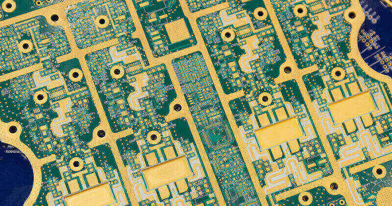
6-Layer High Frequency PCB: Stack and Materials Why Six Layers Is the Common Answer A high frequency design that also has digital and power circuitry tends to end up at six layers. Two layers cannot give the radio frequency section a ground plane and the digital section a separate return;…
Continue Reading
ENIG PCB surface finish macro

PCB Breakaway Tab Size: Strong Enough and Easy to Break

  • By 杰夫
  • 2026年 9月 12日
  • PCB Assembly
  • No Comments
PCB Breakaway Tab Size: Strong Enough and Easy to Break Electronics manufacturing has become a discipline of small details. Solder paste volumes, placement accuracy, temperature profiles and inspection limits all add up to the final result. This guide looks at PCB breakaway tab size from the perspective of a PCBA…
Continue Reading

Nickel Flash Gold PCB: A Thin Gold Finish Explained

  • By Frank guo
  • 2026年 9月 12日
  • PCB Assembly
  • No Comments
Nickel Flash Gold PCB: A Thin Gold Finish Explained What the Finish Actually Is Nickel flash gold is a plated finish of nickel with a very thin layer of gold on top, applied by the same electrochemical sequence used for electroless nickel immersion gold but with a much shorter gold…
Continue Reading

PCB Mouse Bite Design: Small Tabs That Hold the Board

  • By 杰夫
  • 2026年 9月 12日
  • PCB Assembly
  • No Comments
PCB Mouse Bite Design: Small Tabs That Hold the Board Buyers and engineers often focus on the finished product and forget the production line behind it. In practice, most field failures can be traced back to process decisions made during assembly. Understanding PCB mouse bite design gives you a practical…
Continue Reading
PCB Additive Manufacturing vs. Traditional PCB Prototyping

16-Layer PCB: Stack-Up and Manufacturing Limits

  • By Frank guo
  • 2026年 9月 12日
  • PCB Assembly
  • No Comments
16-Layer PCB: Stack-Up and Manufacturing Limits What Changes at Sixteen Layers A sixteen layer board differs from a twelve layer board by more than four layers. The board is thicker, the through vias are longer, the accumulated registration error across the stack is larger, and the number of process passes…
Continue Reading

PCB V-score Depth Tolerance: Scoring the Board for Breaking

  • By 杰夫
  • 2026年 9月 12日
  • PCB Assembly
  • No Comments
PCB V-score Depth Tolerance: Scoring the Board for Breaking Buyers and engineers often focus on the finished product and forget the production line behind it. In practice, most field failures can be traced back to process decisions made during assembly. Understanding PCB V-score depth tolerance gives you a practical advantage…
Continue Reading
PCB Assembly

Standard MCPCB Thickness: How to Choose

  • By Frank guo
  • 2026年 9月 12日
  • PCB Assembly
  • No Comments
Standard MCPCB Thickness: How to Choose Two Thicknesses, One Confusion A metal core board has a metal base and a dielectric layer, and both have a thickness. When a specification says 1.6 millimetres it usually means the total, but the number that governs the thermal performance is the dielectric, and…
Continue Reading
Surface of a laminated panel showing visible glass weave

12-Layer PCB: Stack-Up, Design and Manufacturing

  • By Frank guo
  • 2026年 9月 12日
  • PCB Assembly
  • No Comments
12-Layer PCB: Stack-Up, Design and Manufacturing What Twelve Layers Buys A twelve layer board is the point at which the design has stopped being an exercise in routing and become an exercise in planning. A circuit that needs twelve layers usually has several high speed interfaces, more than one supply…
Continue Reading

PCB Punch Die Clearance: The Gap in the Tool

  • By 杰夫
  • 2026年 9月 12日
  • PCB Assembly
  • No Comments
PCB Punch Die Clearance: The Gap in the Tool Electronics manufacturing has become a discipline of small details. Solder paste volumes, placement accuracy, temperature profiles and inspection limits all add up to the final result. This guide looks at PCB punch die clearance from the perspective of a PCBA factory…
Continue Reading

PCB Leads and Wires: Selection and Termination

  • By Frank guo
  • 2026年 9月 12日
  • PCB Assembly
  • No Comments
PCB Leads and Wires: Selection and Termination The Connection Everyone Forgets Most of a design review is spent on the circuit, and the connection between the board and the rest of the product is treated as a detail. It is not. A solder joint between a stranded wire and a…
Continue Reading
1 … 1,280 1,281 1,282 … 1,623

Search Posts

Categories

  • Electronic Materials
  • Electronical Engineering
  • Industrial Control
  • PCB Assembly
  • PCB Design
  • PCB Manufacturing

Recent Posts

How to Find Faulty Components on a PCB: PCB Design & PCB Manufacturing Guide

How to Find Faulty Components on a PCB: PCB Design & PCB Manufacturing Guide

Jelly - 2026年 9月 25日
How to Check if a PCB Is Working: PCB Design & PCB Manufacturing Guide

How to Check if a PCB Is Working: PCB Design & PCB Manufacturing Guide

Jelly - 2026年 9月 25日
How to Test a PCB: PCB Design & PCB Manufacturing Guide

How to Test a PCB: PCB Design & PCB Manufacturing Guide

Jelly - 2026年 9月 25日

Tags

AOI inspection automotive electronics automotive PCBA quality automotive standards box build assembly component mounting component procurement component supplier conformal coating defect prevention DFM checks DFM review e-bom management electronic component shortage electronic manufacturing services electronic manufacturing standards Electronic Materials electronics design best practice electronics manufacturing capacity electronics sourcing high volume production industrial electronics insertion mount manufacturability review mass production quality mixed technology PCB PCBA inspection PCBA prototype PCBA turnkey PCBA volume pricing PCB Design PCB layout rules PCB Manufacturing PCB sourcing power electronics PCB printed circuit board prototype quick turn PCB reflow soldering SMT assembly quality SMT production solder paste inspection solder paste printing surface mount technology vehicle electronics wave soldering
GOPCBA-logo

As a professional China PCB assembly manufacturer, we provide a full range of electronic manufacturing services from PCB fabrication, PCBA to OEM/ODM, including PCB design, PCB layout, rapid PCBA prototyping, components procurement, SMT/ THT assembly, china pcb assembly, china pcb prototype, PCBA testing and box build assembly.

Linkedin Facebook-f X-twitter Youtube Instagram

PCB ASSEMBLY

  • Prototype PCB Assembly
  • Low Volume PCB Assembly
  • High Volume PCB Assembly
  • Turnkey PCB Assembly
  • SMT PCB Assembly
  • Through-Hole PCB Assembly
  • Mixed Technology PCB Assembly
  • Flex PCB Assembly

OUR SERVICES

  • PCB Design/Layout
  • PCB Manufacturing
  • Rapid PCBA Prototyping
  • Components Procurement
  • Conformal Coating
  • PCBA Testing
  • Box Build Assembly
  • Wire & Cable Harness Assembly

TECHNICAL SUPPORT

  • About Us
  • Quality Management
  • Artificial Intelligence PCBA
  • Industrial PCBA
  • IOT PCBA
  • Medical PCBA
  • Energy PCBA
  • Telecommunications PCBA

Copyright © 2026. Shenzhen Kingda Electronics Co., LTD  All rights reserved. 

  • Sitemap
  • Terms of Service
  • Privacy Policy
Zmdi Zmdi-email Phone-square Whatsapp Weixin
x

ABOUT US

Progressively maintain extensive infomediaries via extensible nich. Capitalize on low hanging fruit. a ballpark value added is activity to beta test. Override the digital divide with additional click throughs from fruit.

LOCATIONS

map

New York Office

+07 554 332 322
contact@example.com
office@example.com
37 San Fairport, NY 14450, New York City
All Locations

FOLLOW US