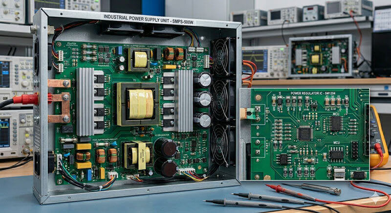
Motor Driver PCB Layout and Current Path Planning A motor driver switches large currents in a few nanoseconds, and the layout decides whether that energy stays in the intended loop or couples into everything nearby. The difference between a quiet driver and one that trips its own protection or upsets…
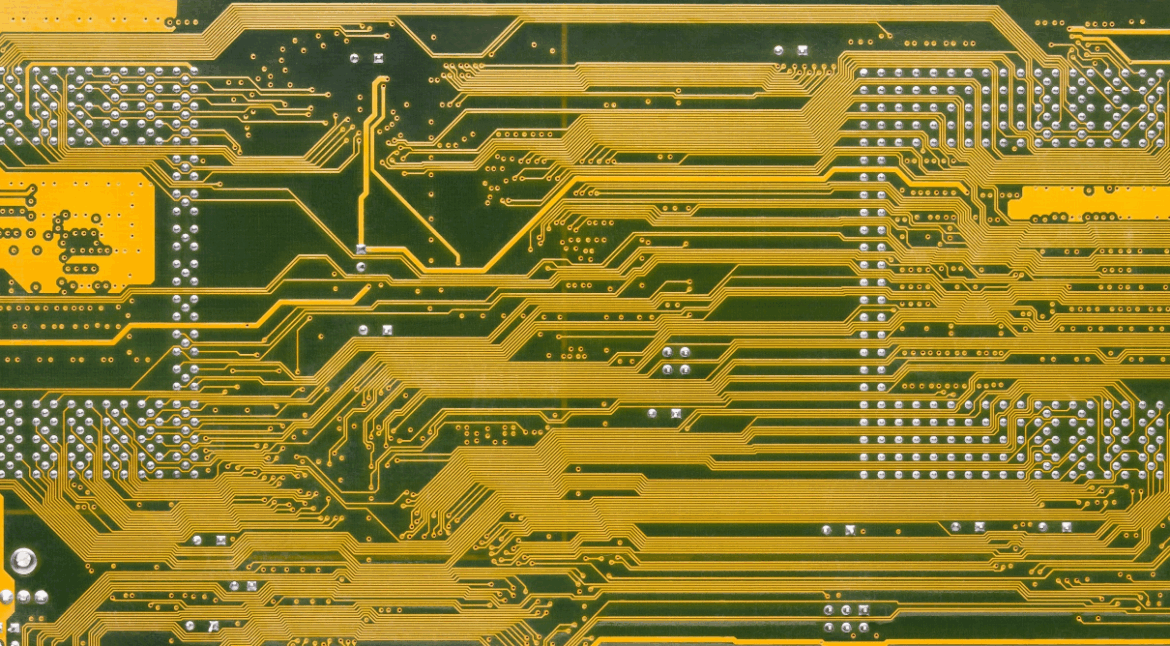
Nitrogen Reflow And Oxygen Concentration Control A reflow oven is normally filled with air, and the oxygen in that air reacts with the solder, the pads and the flux while the joint is being formed. Replacing the atmosphere with nitrogen reduces that reaction, and the result is better wetting, fewer…
Solder Bridging Causes And Process Fixes A bridge is a connection of solder between two conductors that should be separate. On a fine pitch package it is a single deposit that has spread across the gap; between a lead and a neighbouring pad it is a thread formed as the…
Impedance Controlled Connector Launch Design for High Speed A high speed link is usually designed as a clean transmission line, and then it has to pass through a connector. The launch, meaning the transition from the board traces into the connector footprint and out again, is where most of the…
Copper to Board Edge Clearance Rules in PCB Layout A board is cut out of a panel by a router or a punch, and both operations are less precise than the imaging that created the copper. Keeping copper away from the outline is what prevents a routed trace from shorting…
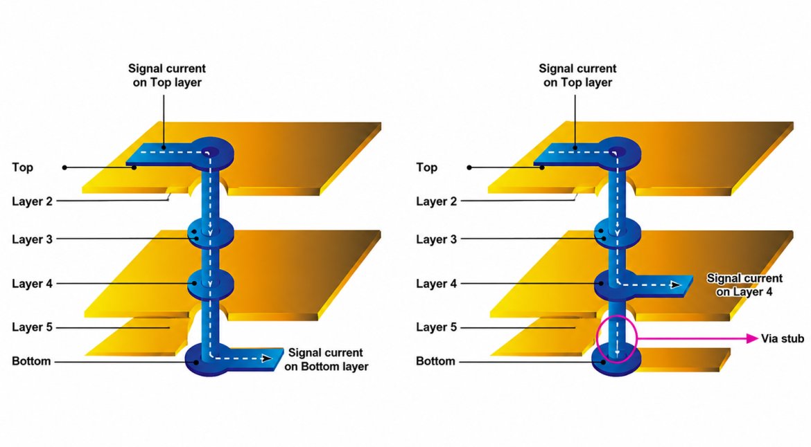
Via Barrel Fatigue Design Guide A via barrel is a copper tube inside a laminate, and the laminate expands about five times as much as the copper in the thickness direction. Every temperature cycle therefore pushes and pulls the barrel, and after enough cycles a crack starts at the corner…
Depanelization Stress And Component Cracking The moment a board is broken out of its panel is the moment it sees the largest mechanical load of its life. The laminate is bent to shear the tabs or to snap the scored web, and that bend travels through the board to every…
PCB Data Package Requirements Guide A PCB data package is the set of files and drawings that a fabricator needs to build the board. It is easy to send too little and it is expensive to send too much in the wrong form. A package that leaves a question open…
Microvia Reliability Design Guide A microvia is a small hole, usually below 0.15 mm in diameter, that connects two adjacent layers in a high density board. It is drilled with a laser rather than with a mechanical bit, and it is the feature that allows a fine pitch device to…
Test Point Design For In Circuit Test Fixtures In circuit test works by pressing a bed of nails against the underside of the board and measuring each net. The nails are spring loaded probes, and each one has to land on a surface that is flat, clean, of a known…