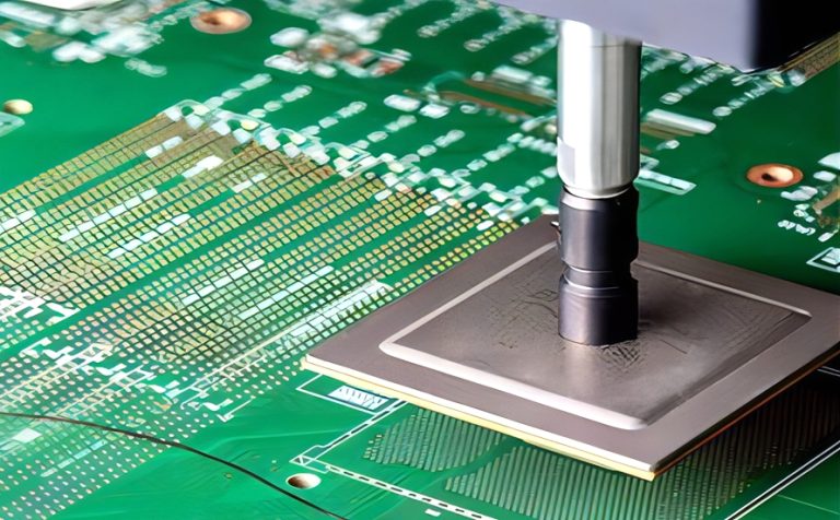
Panel Cleaning Before Lamination and Coating Steps Between the plating line and the lamination press, and again before solder mask is applied, the panel has to be clean. Contamination at those points does not show up immediately: it appears later as a delaminated inner layer, a lifted mask or a…
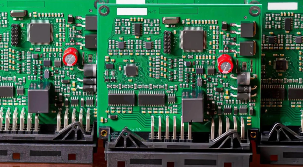
Design For Testability: Design Rules and Process Limits Design for testability is the practice of making a board easy to verify. It is a layout decision that is made once, early, and that decides whether the product can be tested in a minute or debugged for an hour. A design…
Gold Finger Chamfer And Bevel Depth Control A gold finger edge connector works by sliding. The board is pushed into a socket, and the leading edge of the board has to guide itself between the contacts without catching on them, without bending a contact spring and without removing metal from…
Embedded Copper Coin PCB Design in 5G Base Station Power Amplifier Heat Dissipation 5G base station RF power amplifier modules, or PA, experience significant junction temperature rise under high-frequency and high-power operating conditions. Typical GaN HEMT devices can exceed 150 degrees Celsius junction temperature at 3.5 GHz band and 30…
Tombstoning And The Forces That Lift A Chip A two terminal chip component can lift onto one end during reflow and stand on its termination like a headstone. The defect is called tombstoning, it happens within a second or two at the moment the solder becomes liquid, and it is…
PCB Storage Humidity Control Guide A finished printed circuit board is not inert. The laminate absorbs moisture from the air, the surface finish reacts with the atmosphere, and a board that has been stored badly will fail during the reflow soldering that was supposed to be the easy part. PCB…
Design of Experiments for PCB Process Optimisation Process problems rarely have a single cause. Changing one parameter at a time, which is how most process work is done, cannot reveal what happens when two parameters are changed together, and it is inefficient when several parameters need to be explored. Design…
PCB Dewarping Process Guide A board that has bowed or twisted cannot be assembled reliably. The paste printer cannot hold it flat, the placement machine sees a shifting fiducial and the reflow oven bakes the distortion in. Dewarping is the process that removes the shape after the board has been…
Stencil Aperture Design And Paste Release The stencil is the only part of the printing process that decides how much solder paste lands on each pad, and the aperture design is what the stencil maker actually cuts. Every joint on the board, and therefore every solder fillet, void, bridge and…
Tdr Impedance Measurement: Design Rules and Process Limits A TDR impedance measurement sends a fast edge down a trace and watches the reflection that comes back. The reflection is a picture of the impedance along the line, so the instrument shows the trace, the via, the connector and the pad…