KingdaKingdaKingda

Call Us 24/7

+86-181-2376-9076

Send Us Mail

sales@gopcba.com

Our Location

Baoan District, Shenzhen, China

Language

  • enEnglish
    • fr France
    • itItalian
Kingda
  • Home
  • PCB Assembly
    • Prototype PCB Assembly
    • Turnkey PCB Assembly
    • Low Volume PCB Assembly
    • High Volume PCB Assembly
    • SMT PCB Assembly
    • Through-Hole PCB Assembly
    • Mixed Technology PCB Assembly
    • Flex PCB Assembly
  • Services
    • PCB Design/Layout
    • PCB Manufacturing
    • Rapid PCBA Prototyping
    • Components Procurement
    • Conformal Coating
    • PCBA Testing
    • Box Build Assembly
    • Wire & Cable Harness Assembly
  • Industry Solutions
    • Medical PCBA
    • Telecommunications PCBA
    • Energy PCBA
    • Industrial PCBA
    • Artificial Intelligence PCBA
    • IOT PCBA
  • Resources
    • PCB Capabilities
    • PCBA Capabilities
    • FAQ
    • Blog
  • About Us
    • About Us
    • Why Us
    • Quality Management
  • Contact Us
Get A Quote
zuzhuang1-1

DC-DC Layout and Routing Points for Switching Converters

  • By Frank guo
  • 2026年 9月 13日
  • PCB Assembly
  • No Comments
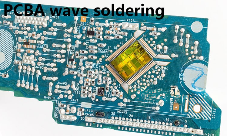
DC-DC Layout and Routing Points for Switching Converters A switching converter is a small circuit with large currents, and the board around it is part of the circuit. The loop that carries the switching current has inductance that the schematic does not show, and every millimetre of it contributes to…
Continue Reading
op1

PCB Layout: Placement and Routing Practice

  • By Frank guo
  • 2026年 9月 13日
  • PCB Assembly
  • No Comments
PCB Layout: Placement and Routing Practice PCB layout is where a schematic becomes a piece of hardware, and most of the problems that appear during bring up were decided on the screen rather than in the fabrication shop. Placement sets the shape of every current path on the board, the…
Continue Reading
医疗电子可持续性

Solder Void Formation and Vacuum Reflow

  • By Frank guo
  • 2026年 9月 13日
  • PCB Assembly
  • No Comments
Solder Void Formation and Vacuum Reflow Voids in a solder joint come from gas that cannot escape before the solder solidifies. The gas can come from the paste, from the plating or from the surfaces, and the way to remove it is to make it easier to leave. Where the…
Continue Reading
High-Frequency PCB Design

Load Cell Amplifier Gain Selection

  • By Frank guo
  • 2026年 9月 13日
  • PCB Assembly
  • No Comments
Load Cell Amplifier Gain Selection A load cell converts a force into a small differential voltage, and the amplifier that follows decides how much of that voltage the system can actually use. Gain selection is not a single number: it depends on the full scale output of the bridge, the…
Continue Reading
55387056_2

Drill Registration and Layer-to-Layer Alignment Control

  • By Frank guo
  • 2026年 9月 13日
  • PCB Assembly
  • No Comments
Drill Registration and Layer-to-Layer Alignment Control Holes rarely land exactly where the artwork intended them to. Every layer is imaged, etched, laminated and drilled with its own small errors, and the hole must still land inside the pad on every layer it passes through. Registration is the discipline of keeping…
Continue Reading
Ceramic PCB

Engineering Change Orders in PCB Production

  • By Frank guo
  • 2026年 9月 13日
  • PCB Assembly
  • No Comments
Engineering Change Orders in PCB Production A change order is a small document with a large effect. It invalidates drawings, programs, fixtures, test limits and stock, and it does so in several places at once. The cost of a change is rarely in the change itself. What a Change Order…
Continue Reading
pin11-min

ENIG Process Control: Electroless Nickel Immersion Gold

  • By Frank guo
  • 2026年 9月 13日
  • PCB Assembly
  • No Comments
ENIG Process Control: Electroless Nickel Immersion Gold Electroless nickel immersion gold is the finish of choice for fine pitch, for wire bonding and for boards that will be stored for a long time before assembly. It is also the finish with the narrowest process window, because the nickel layer is…
Continue Reading
PCB Assembly

Via in Pad for BGA Fanout: Process and Design Points

  • By Frank guo
  • 2026年 9月 13日
  • PCB Assembly
  • No Comments
Via in Pad for BGA Fanout: Process and Design Points A via in pad places the connection directly in the centre of a surface mount land instead of beside it. On a fine pitch ball grid array the pads are already close together and the escape routing between them is…
Continue Reading
Flexible PCB

Placement Nozzle: Design Rules and Process Limits

  • By Frank guo
  • 2026年 9月 13日
  • PCB Assembly
  • No Comments
Placement Nozzle: Design Rules and Process Limits The only part of a placement machine that touches the component is the nozzle, and the entire accuracy of the machine passes through it. A nozzle that is the wrong size for the part produces a pick up that is off centre, a…
Continue Reading
Flexible PCB

Reflow of Assemblies With Mixed Thermal Mass

  • By Frank guo
  • 2026年 9月 13日
  • PCB Assembly
  • No Comments
Reflow of Assemblies With Mixed Thermal Mass A board that carries a heavy connector, a thick copper plane and a small chip component on the same side does not heat evenly. The profile that satisfies one of them will not satisfy the other, and the compromise decides the yield. Why…
Continue Reading
1 … 800 801 802 … 1,626

Search Posts

Categories

  • Electronic Materials
  • Electronical Engineering
  • Industrial Control
  • PCB Assembly
  • PCB Design
  • PCB Manufacturing

Recent Posts

Surface Mount Technology (SMT): Process, Components, Design Guidelines & PCB Assembly

Surface Mount Technology (SMT): Process, Components, Design Guidelines & PCB Assembly

Zane Zhang - 2026年 10月 2日
Cheap PCB Costs: PCB Design, PCB Manufacturing & SMT vs TH Guide

Cheap PCB Costs: PCB Design, PCB Manufacturing & SMT vs TH Guide

Jelly - 2026年 9月 30日
Cheap PCB Costs: PCB Design, PCB Manufacturing & SMT vs TH Guide

Cheap PCB Costs: PCB Design, PCB Manufacturing & SMT vs TH Guide

Jelly - 2026年 9月 30日

Tags

AOI inspection automotive electronics automotive PCBA quality automotive standards box build assembly component mounting component procurement component supplier conformal coating defect prevention DFM checks DFM review e-bom management electronic component shortage electronic manufacturing services electronic manufacturing standards Electronic Materials electronics design best practice electronics manufacturing capacity electronics sourcing high volume production industrial electronics insertion mount manufacturability review mass production quality mixed technology PCB PCBA inspection PCBA prototype PCBA turnkey PCBA volume pricing PCB Design PCB layout rules PCB Manufacturing PCB sourcing power electronics PCB printed circuit board prototype quick turn PCB reflow soldering SMT assembly quality SMT production solder paste inspection solder paste printing surface mount technology vehicle electronics wave soldering
GOPCBA-logo

As a professional China PCB assembly manufacturer, we provide a full range of electronic manufacturing services from PCB fabrication, PCBA to OEM/ODM, including PCB design, PCB layout, rapid PCBA prototyping, components procurement, SMT/ THT assembly, china pcb assembly, china pcb prototype, PCBA testing and box build assembly.

Linkedin Facebook-f X-twitter Youtube Instagram

PCB ASSEMBLY

  • Prototype PCB Assembly
  • Low Volume PCB Assembly
  • High Volume PCB Assembly
  • Turnkey PCB Assembly
  • SMT PCB Assembly
  • Through-Hole PCB Assembly
  • Mixed Technology PCB Assembly
  • Flex PCB Assembly

OUR SERVICES

  • PCB Design/Layout
  • PCB Manufacturing
  • Rapid PCBA Prototyping
  • Components Procurement
  • Conformal Coating
  • PCBA Testing
  • Box Build Assembly
  • Wire & Cable Harness Assembly

TECHNICAL SUPPORT

  • About Us
  • Quality Management
  • Artificial Intelligence PCBA
  • Industrial PCBA
  • IOT PCBA
  • Medical PCBA
  • Energy PCBA
  • Telecommunications PCBA

Copyright © 2026. Shenzhen Kingda Electronics Co., LTD  All rights reserved. 

  • Sitemap
  • Terms of Service
  • Privacy Policy
Zmdi Zmdi-email Phone-square Whatsapp Weixin
x

ABOUT US

Progressively maintain extensive infomediaries via extensible nich. Capitalize on low hanging fruit. a ballpark value added is activity to beta test. Override the digital divide with additional click throughs from fruit.

LOCATIONS

map

New York Office

+07 554 332 322
contact@example.com
office@example.com
37 San Fairport, NY 14450, New York City
All Locations

FOLLOW US