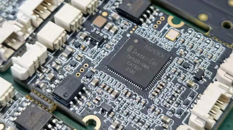
HDI Blind and Buried Via Process Chain Explained High density interconnect design solves the problem of routing a dense board in limited space. The blind and buried via structures that make it possible are produced by a process chain in which each step has a narrow window, and a deviation…
Metallizing Aluminium Nitride Substrates Aluminium nitride occupies a specific niche among substrate materials. It is a ceramic that is electrically insulating and thermally conductive, and it is chosen when a circuit has to move a large amount of heat through an insulating layer rather than around it. The material itself…
Microvia: Design Rules and Process Limits Microvias are the feature that makes high density interconnect possible, and they are also the feature with the least tolerance for process variation. Understanding how they are made explains why the design rules around them are stricter than for a conventional through hole. How…
Layer Stack: Manufacturable Design: Decisions That Belong Up Front Casting a design in the language of a manufacturing process forces a level of precision that a schematic review does not, and the exercise usually finds something. The items below are the ones that most often turn out to be decided…
Reactance And Impedance Explained For Board Design Resistance, capacitance and inductance are the three properties that describe how a circuit responds to a signal, and impedance is the term that combines them. On a board the distinction matters because a component that looks like a small capacitance on a schematic…
Four Layer Flex and Rigid Flex Boards Flexible circuits are used because they bend, and bending is exactly what limits how many layers they can carry. A four layer flex is routine in modern designs, but it is a different construction from a two layer flex with extra copper, and…
Copper Pour and Via Connection Rules for PCB Layout Copper pour is one of the last steps in a layout and one of the easiest places to introduce a defect, because the connection between the pour and every via, pad and plane is controlled by rules rather than by the…
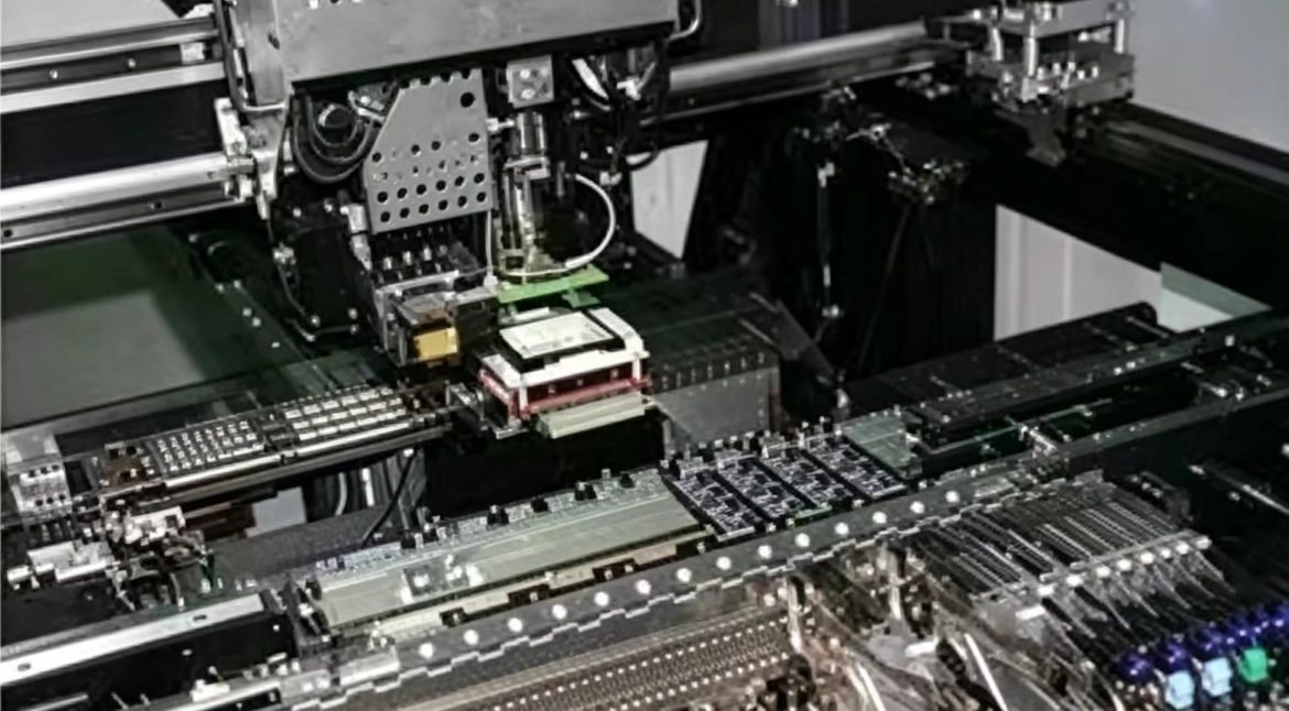
Reflow Profile: Reflow Profiling: Measuring What the Solder Sees Thermal profiling is the measurement that connects a reflow oven’s settings to what the solder actually experiences, and it is the only way to know whether a profile is suitable for a particular assembly. The oven’s display shows the air temperature,…
Drill Bit Life and Regrind Control in PCB Drilling Every hole in a circuit board is cut by a carbide tool that is wearing from the moment it touches the stack. The wear shows up as a change in hole diameter, a rougher wall, and eventually as a smear or…
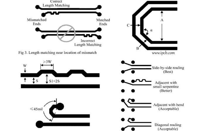
Fiber Weave Skew in Differential Pair Routing A differential pair is supposed to arrive at the receiver with both traces carrying the same signal at the same time. On a real board the two traces often see slightly different dielectric material, because the laminate is not homogeneous. The fiber weave…