Ground Bounce: Design Rules and Process Limits A single output switching produces a clean waveform, and the same device with an entire bus toggling at once produces intermittent receiver errors. The ground net is continuous, a multimeter reads a fraction of an ohm between the chip ground pin and the…
Industrial Control HDI PCB Cost: Layers, Vias and Volume Industrial control boards are moving to HDI for the same reason consumer boards did, but with an added constraint: the product has to last fifteen years in a cabinet that vibrates and heats. That combination changes which HDI techniques are worth…
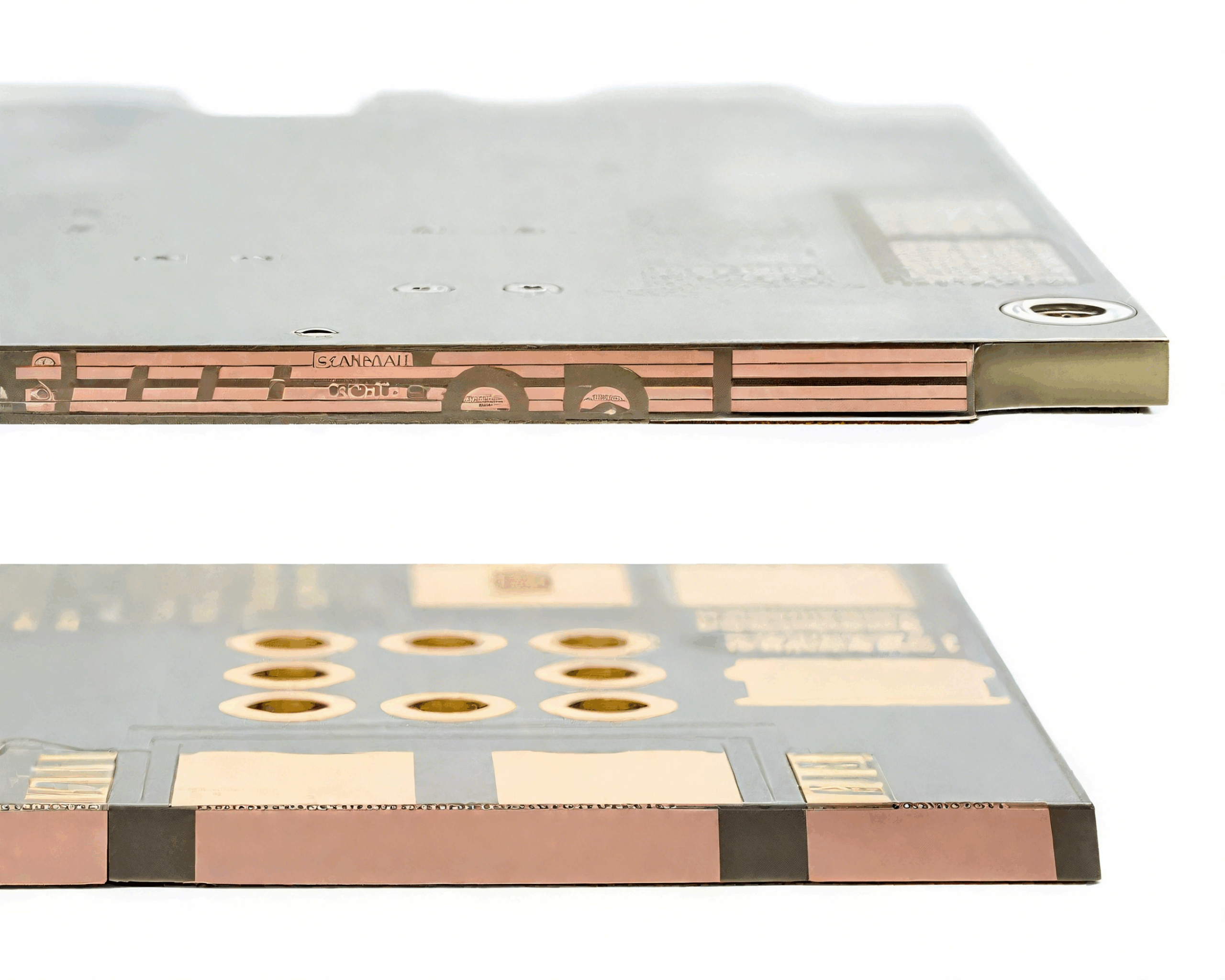
Heavy Copper PCB Design: A DFM Checklist Heavy copper boards are built for current, not for density, and the design rules that work on a conventional board do not survive the transition. Foil that is two or four times thicker etches differently, drills differently and behaves differently under solder mask,…
Thermal Via: Thermal Path Design From Junction to Ambient Heat is the enemy of every electronic product up to a point, and beyond that point it is the friend. Most failures in service are thermal in origin, and most of them are decided by the path the heat takes from…
Signal And Power Integrity Analysis Basics Signal integrity and power integrity are usually treated as two subjects, and on a board they are one. A driver switches current out of the power distribution network and back into it through the ground plane, and the quality of that supply at the…
How Drilling Defects Ruin a PCB A drilled hole is the most heavily loaded feature on a printed circuit board. It interrupts the laminate, it has to be plated uniformly through its entire depth, and it has to survive thermal cycling for the life of the product. When drilling defects…
PCB Copper Surface Condition and Wetting Behaviour Copper on a finished board is not flat. The surface is a series of peaks and valleys created by the lamination texture, the plating and the etching, and every soldering process has to cope with that topography. Understanding where the roughness comes from…
DC-DC Inductor Placement and Radiated Emissions A switching supply that fails radiated emissions is usually attacked by changing the inductor, adding filter capacitors and improving the ground plane. Those measures address the symptoms, and they often produce only a few decibels of improvement. In one representative case, a 60 volt…
Thermal Fatigue and Solder Joint Life Prediction A solder joint rarely fails because it was made badly. It fails because it was cycled between two temperatures thousands of times, and each cycle stretched and compressed it a little more. Thermal fatigue is the dominant wear-out mechanism for electronics in automotive,…
Fuse Traces and Overcurrent Protection on PCBs A fuse trace is a deliberate weak point: a short, narrow section of copper that melts before the rest of the circuit is damaged. It costs nothing, needs no component, and fails more predictably than many engineers expect. It also has to be…