IC Substrate PCB: Build-up Layers and Fine Line Technology An IC substrate sits between a bare die and the board it is mounted on, and it is closer to a semiconductor product than to a printed circuit. Its conductors are measured in single-digit micrometres, its vias are formed by laser,…

High Speed PCB Design for DSP Systems: Noise Control A DSP runs at high clock rates with fast edges, and a fast edge is what makes a board behave like a transmission line rather than a set of connections. The interference problems that appear in a working system come mostly…
Fabrication Data Pitfalls That Delay a Prototype Fabrication data problems are rarely caused by a design being wrong. They are caused by the data being ambiguous, and the cost appears as a query from the fabricator, a delay in the schedule or a panel that has to be reworked. Most…
Power Supply Design on a PCB: Requirements and Layout Priorities Power supply design on a PCB is judged by two things that the schematic cannot express: whether the switching current stays inside the loop that was planned for it, and whether the copper that carries it is wide enough to…
Capacitor Behaviour and What It Means on a PCB A capacitor is the simplest component in the circuit and the one whose behaviour is most often taken for granted. It stores charge, it resists a change in voltage, and it passes a changing signal while blocking a steady one. Every…
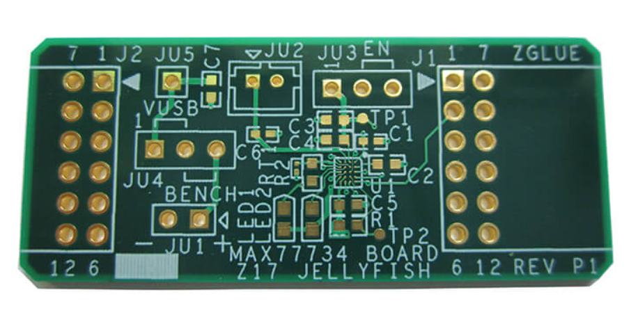
PCB Silkscreen Readability: Writing on the Board Modern electronics depend on boards that are assembled correctly the first time. Every product – a phone, a charger, a medical instrument or an industrial controller – relies on thousands of solder joints that must conduct current for years. This article explains PCB…
PCB Legend Over Pads: When the Ink Has to Move Buyers and engineers often focus on the finished product and forget the production line behind it. In practice, most field failures can be traced back to process decisions made during assembly. Understanding PCB legend over pads gives you a practical…
PCB Design Process: From Netlist to Fabrication Data A board that is easy to build, easy to test and easy to service is almost always the result of a disciplined PCB design process rather than a clever one. The process produces two things: a layout that satisfies the electrical intent,…
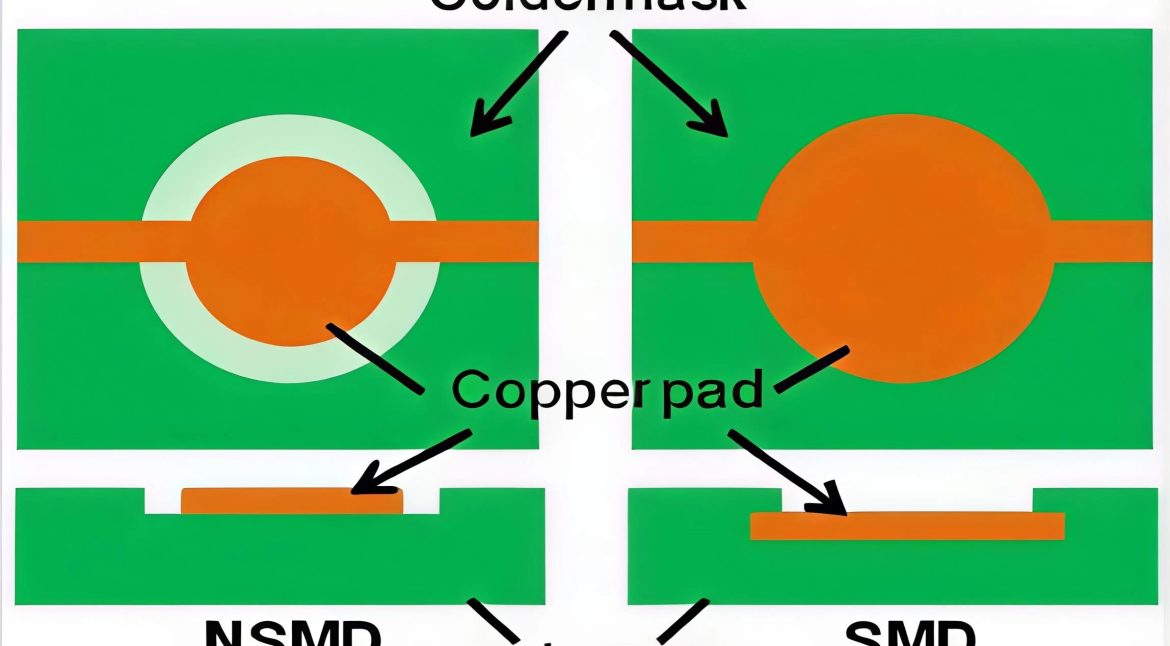
PCB Mask Dam Width: The Wall Between Pads Electronics manufacturing has become a discipline of small details. Solder paste volumes, placement accuracy, temperature profiles and inspection limits all add up to the final result. This guide looks at PCB mask dam width from the perspective of a PCBA factory floor,…
PCB Silver Finish Tarnish: A Bright Pad That Fades Electronics manufacturing has become a discipline of small details. Solder paste volumes, placement accuracy, temperature profiles and inspection limits all add up to the final result. This guide looks at PCB silver finish tarnish from the perspective of a PCBA factory…