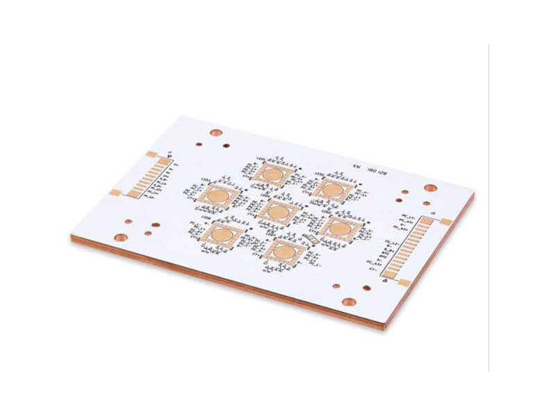
PCB Edge Plating: EMI Shielding and Grounding Most of a circuit board is designed on its faces, with the edges treated as a cutting line. Edge plating changes that by putting conductor on the edge itself, connecting the outer layers and sometimes the inner ground planes around the perimeter of…
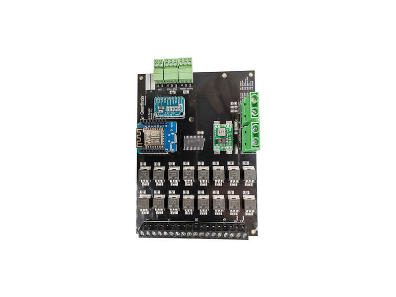
Schematic Entry Mistakes That Break the Netlist The schematic is the source of truth for the whole project. Every net in the layout, every entry in the bill of materials and every test point in the netlist comes from it, so a small inconsistency at the schematic stage propagates into…
Core PCB Design Issues and How to Resolve Them Board failures rarely come from a clever circuit that did not work. They come from a handful of recurring issues that appear in almost every design: a sensitive part placed next to a heat source, a plane that turned into a…
PCB Wire Gauge Selection: Picking the Right Wire Buyers and engineers often focus on the finished product and forget the production line behind it. In practice, most field failures can be traced back to process decisions made during assembly. Understanding PCB wire gauge selection gives you a practical advantage when…
PCB Keyed Connector Selection: Right Plug, Wrong Hole Electronics manufacturing has become a discipline of small details. Solder paste volumes, placement accuracy, temperature profiles and inspection limits all add up to the final result. This guide looks at PCB keyed connector selection from the perspective of a PCBA factory floor,…
OSP versus ENIG: Choosing a PCB Surface Finish Every exposed copper pad on a board has to be protected between fabrication and soldering, and the coating that does that job is called the surface finish. The choice looks like a detail until a production line starts rejecting joints or a…
Surface Mount Assembly versus Through Hole: How to Choose The choice between surface mount and through hole technology is no longer a question of which process is modern. Both are mature, both are used in high reliability products, and most boards today carry a mixture of the two. The decision…
PCB Design Constraints That Survive Manufacturing Most PCB teams still hand down design rules as a table of fixed numbers: a minimum trace width here, a clearance there, a target impedance for every net on a given layer. That table works until the board stops being simple. Once a design…
Power Supply PCB Layout: Loop Area, Ground and Safety A switching power supply is not one circuit. It is at least three circuits sharing a board: the high-current power stage, the gate drive that controls it, and the small-signal sensing that decides what the power stage should do. Treating them…
PCB Stepped Slot and Cavity: Depth Control and Design Rules A stepped slot is a recess milled into a board to a controlled depth rather than through the whole panel. The floor of the recess becomes a mounting surface, a light path or the seat for a module that has…