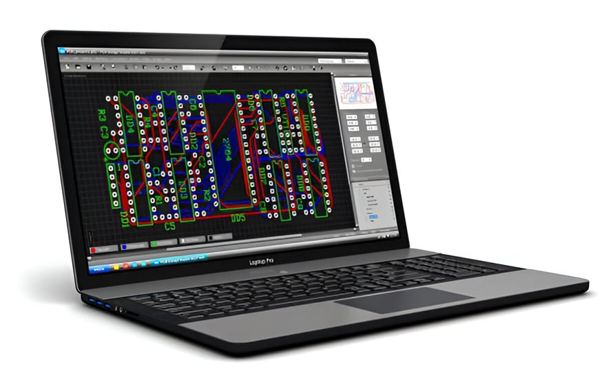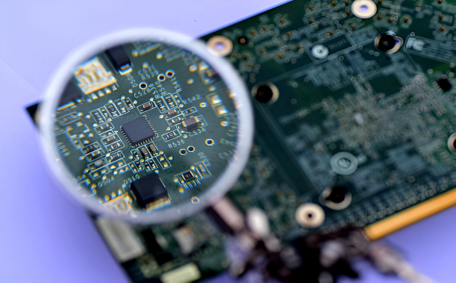
PCB Panelization for SMT Assembly: Complete Design Guide In modern electronics manufacturing, PCB panelization is widely used to improve production efficiency, reduce handling time, and optimize manufacturing costs. Instead of processing every individual printed circuit board separately, multiple PCB units can be combined into a larger manufacturing panel and…
How to Prevent FPC Pad Lift-Off: 8 Design Methods for Better Pad Adhesion FPC pads provide the electrical and mechanical interface between a flexible circuit and electronic components or external wires. However, because an FPC uses a thin and flexible substrate, its copper pads can be more vulnerable to…
PCB Via vs. Pad: Differences, Hole Tolerances, and Design Guidelines When designing a printed circuit board, understanding the difference between a PCB Via and a PCB Pad is essential for achieving reliable electrical performance and smooth manufacturing. Although both can contain holes and connect to copper features, they serve…
How to Design Through-Hole Pads with Copper Exposure on One Side and Solder Mask Coverage on the Other In conventional PCB design, through-hole components are generally designed with solderable copper pads exposed on both sides of the circuit board. However, some applications require a through-hole pad to be soldered…
FPC Tear Prevention Line: Purpose, Design Requirements, and Best Practices Flexible printed circuits are widely used in compact and lightweight electronic products because they can bend, fold, and fit into irregular mechanical spaces. However, their thin and flexible structure also creates unique challenges during manufacturing and depanelization. Unlike rigid…
FPC-to-PCB Connections: 7 Common Methods Explained How Does FPC Connect to PCB? As electronic products become smaller, thinner, and more integrated, FPC to PCB connection technology has become increasingly important. A Flexible Printed Circuit (FPC) provides lightweight construction, flexibility, and three-dimensional routing, while a rigid PCB provides mechanical support, component…
SMT Flying Probe Testing: Process, Capabilities, Limitations, and Benefits What Is SMT Flying Probe Testing? SMT Flying Probe Testing is an electrical testing method used during surface mount technology (SMT) production to verify PCB assembly quality, component connections, and circuit integrity. Unlike traditional ICT systems that use a fixed bed-of-nails…
How to Panelize PCBs for SMT Assembly In electronics manufacturing, PCB Panelization is the process of combining multiple individual printed circuit boards into a larger production panel. Panelization allows manufacturers to process several boards at the same time during solder paste printing, component placement, reflow soldering, inspection, and other…
PCB Panelization: Process Edge, Tooling Hole and Fiducial Mark Design Guidelines When designing a PCB for automated manufacturing, panelization and positioning features must be considered before production. Properly designed PCB panelization improves board stability during manufacturing, supports accurate positioning during SMT assembly, and reduces the risk of damage during…
PCB Copper Pour: Applications and Manufacturing Considerations PCB copper pour is a common PCB layout and manufacturing technique in which large areas of copper are added to unused regions of a circuit board. Depending on the design, the copper area may be connected to ground, a power network, or…