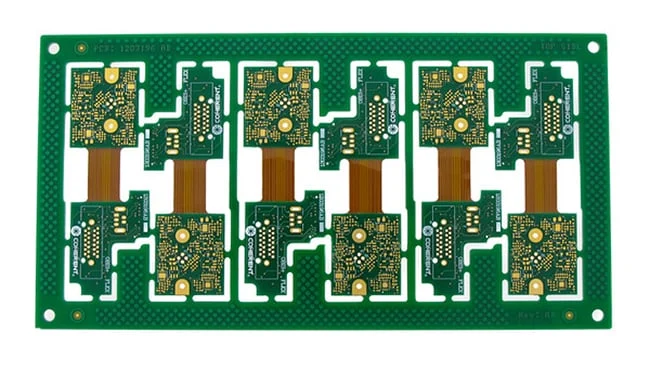


PCB Lamination Process: Materials, Temperature and Pressure What Lamination Does Lamination is the step that turns separate inner layers into one solid multilayer board. The inner layers are stacked with sheets of partially cured resin between them, and the whole stack is pressed under heat and pressure until the resin…
PCB Via Barrel Crack: A Break in the Hole Wall Modern electronics depend on boards that are assembled correctly the first time. Every product – a phone, a charger, a medical instrument or an industrial controller – relies on thousands of solder joints that must conduct current for years. This…
PCB Edge Plating: Complete Guide to Design and Process What PCB Edge Plating Is Edge plating means copper deposited on the cut edge of a printed circuit board. Instead of a bare laminate edge, the board carries a continuous metal surface around part or all of its perimeter. That metal…
SMT Reflow Solder Paste Alloy: The Metal in the Paste Buyers and engineers often focus on the finished product and forget the production line behind it. In practice, most field failures can be traced back to process decisions made during assembly. Understanding SMT reflow solder paste alloy gives you a…
PCB Copper Trace Electromigration: When the Metal Moves Buyers and engineers often focus on the finished product and forget the production line behind it. In practice, most field failures can be traced back to process decisions made during assembly. Understanding PCB copper trace electromigration gives you a practical advantage when…
Blood Glucose Meter PCB: Design, Cost and Manufacturing What a Glucose Meter Board Has to Do A blood glucose meter is a precision instrument in a pocket-sized package. The test strip contains an enzyme that reacts with glucose and produces a tiny electrical current, often in the nanoampere to microampere…
Heavy Copper PCB Price: 2oz, 3oz, 4oz and 6oz Cost Comparison What Counts as Heavy Copper Standard PCB copper is one ounce per square foot, about 35 microns thick. Heavy copper usually means two ounces and above, and it is used when the board has to carry high current, survive…
Via-in-Pad Solder Wicking: Causes and Solutions What Via-in-Pad Means A via-in-pad is a plated hole placed directly in the centre of a component land rather than beside it. The technique frees routing space under dense BGA and QFN packages, shortens the current path and improves thermal transfer, which is why…
PCB Plasma Etching vs Chemical Etching: Which Is Better? Two Ways to Remove Material Almost every PCB process needs to remove material at some point, whether it is copper that must be cleared to define traces, resin smear that must be cleaned out of a drilled hole, or a surface…
Ultrasonic Transducer PCB: Design, Materials and Applications What an Ultrasonic Transducer PCB Does An ultrasonic transducer converts electrical energy into sound and back again. The piezoelectric element does the physical work, but the printed circuit board around it decides how cleanly the signal is delivered and how much of the…