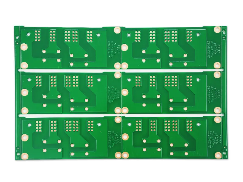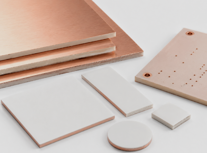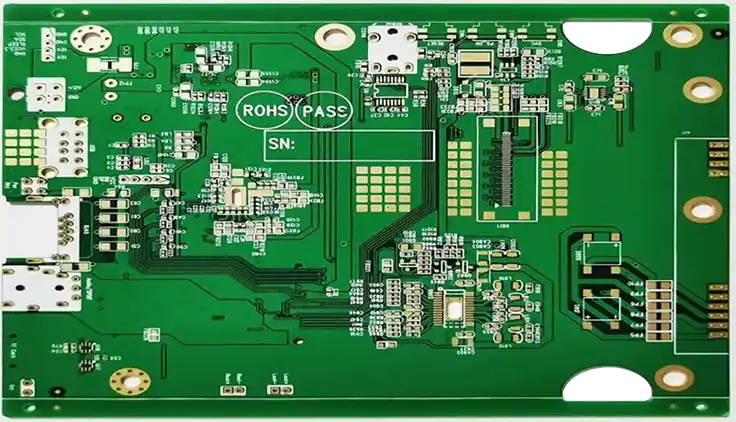


PCB Acidic vs Alkaline Etching: Key Differences What PCB Etching Does Etching is the step that removes unwanted copper from a printed circuit board and leaves the traces behind. After the pattern is defined by a photoresist or a plated metal resist, the board passes through a chemical bath that…
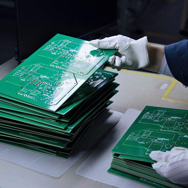
How Many Layers Does a High-Speed PCB Need? What Makes a PCB High Speed A board is high speed when the rise time of its signals is short compared with the trace length, so the interconnect behaves like a transmission line instead of a simple wire. In practice that usually…
PCB Panelization for Assembly: Requirements and Design Rules What PCB Panelization Means Panelization is the process of arranging several identical or mixed circuit boards into one larger panel so that they can be fabricated, printed and assembled as a single unit. Instead of handling tiny boards one at a time,…
Carbon Ink PCB vs Carbon Film PCB: How to Choose Two Carbon Layers on One Board Screen-printed carbon is one of the cheapest ways to add function to a printed circuit board, and two terms appear again and again: carbon ink PCB and carbon film PCB. On the finished board…
PCB Dielectric Withstanding Voltage: The Voltage the Board Can Take Modern electronics depend on boards that are assembled correctly the first time. Every product – a phone, a charger, a medical instrument or an industrial controller – relies on thousands of solder joints that must conduct current for years. This…
SMT Reflow Peak Dwell Time: The Time at the Top Buyers and engineers often focus on the finished product and forget the production line behind it. In practice, most field failures can be traced back to process decisions made during assembly. Understanding SMT reflow peak dwell time gives you a…
PCB Solder Mask Curing: Setting the Mask Hard Modern electronics depend on boards that are assembled correctly the first time. Every product – a phone, a charger, a medical instrument or an industrial controller – relies on thousands of solder joints that must conduct current for years. This article explains…
SMT Component Standoff Height: The Gap Under the Part Electronics manufacturing has become a discipline of small details. Solder paste volumes, placement accuracy, temperature profiles and inspection limits all add up to the final result. This guide looks at SMT component standoff height from the perspective of a PCBA factory…
PCB Copper Trace Skin Effect: When the Signal Runs on the Edge Buyers and engineers often focus on the finished product and forget the production line behind it. In practice, most field failures can be traced back to process decisions made during assembly. Understanding PCB copper trace skin effect gives…
SMT Reflow Solder Joint Inspection: Checking Every Joint Electronics manufacturing has become a discipline of small details. Solder paste volumes, placement accuracy, temperature profiles and inspection limits all add up to the final result. This guide looks at SMT reflow solder joint inspection from the perspective of a PCBA factory…