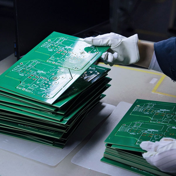
How Many Layers Does a High-Speed PCB Need?
What Makes a PCB High Speed
A board is high speed when the rise time of its signals is short compared with the trace length, so the interconnect behaves like a transmission line instead of a simple wire. In practice that usually means edge rates below a few hundred picoseconds, clock rates above roughly 100 MHz, or interfaces such as DDR, PCIe, USB 3, HDMI, Ethernet and SerDes links. Once a design crosses that line, the layer count stops being a cost decision and becomes a signal integrity decision, because every fast signal needs a clean return path and controlled impedance.
Why Layer Count Matters
Layers give you three things that high-speed design cannot do without: dedicated reference planes, controlled trace geometry and room to route without crossing splits. A two-layer board can carry a fast signal, but its return current has no continuous plane to follow, so impedance is uncontrolled and radiation is high. Adding layers lets you place ground and power planes directly under the signal layers, keep the return path short and predictable, and set the trace width and dielectric spacing that give a target impedance.
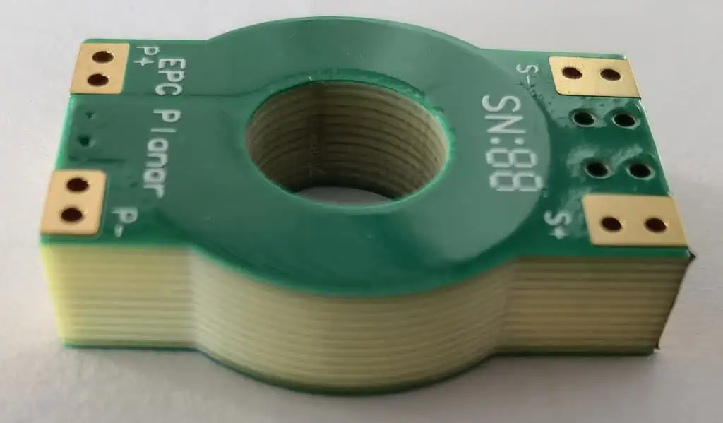
The 4-Layer High-Speed PCB
A four-layer stack-up is usually signal, ground, power and signal. It is the cheapest option that still provides a solid reference plane, and it works well for moderate speeds: microcontroller boards, USB 2.0, 100 Mbit Ethernet, low speed DDR and general mixed-signal designs. The limitation is routing density. With only two signal layers, dense fine pitch packages force long detours, and any plane split under a fast trace creates a return path discontinuity. Four layers are a good fit when the fastest edge rates stay above about 500 picoseconds and the board is not crowded.
The 6-Layer High-Speed PCB
Six layers normally means signal, ground, signal, power, ground, signal. The extra layer gives every fast signal a nearby ground plane and lets you keep high speed traces on inner layers, where they are shielded by copper above and below. This is the practical sweet spot for most high-speed boards: DDR3 and DDR4, Gigabit Ethernet, PCIe Gen2 and Gen3, and mid-range SerDes. Six layers also make it easier to maintain a continuous reference plane and to separate analog, digital and power domains, which helps EMI performance.
The 8-Layer High-Speed PCB
Eight layers are used when the design has many high speed nets, several power rails or very fine pitch devices such as large BGA packages. A typical stack-up keeps ground planes adjacent to every signal layer and dedicates separate layers to power distribution. This gives the lowest crosstalk, the best impedance control and the most routing freedom, and it supports DDR5, PCIe Gen4 and Gen5, 10G and 25G SerDes, and dense backplanes. The cost is real: more layers mean more material, more lamination steps and a longer lead time, so eight layers should be justified by the electrical requirement rather than by habit.

Comparison at a Glance
4 layers. One or two reference planes, moderate speeds, lowest cost, tight routing. 6 layers. Two ground planes and one power plane, good shielding, balanced cost, suits most high speed products. 8 layers. Multiple ground and power planes, best signal integrity, highest cost, used for dense and very fast designs. In every case the fastest signals should reference a solid ground plane, and no high speed trace should cross a plane split.
Reference Planes Drive the Choice
The number of signal layers matters less than the number of reference planes and how they are arranged. Two signal layers separated by one ground plane are far better than four signal layers with a single distant ground. When you plan a stack-up, place a ground plane next to every high speed signal layer, keep the dielectric between them thin to tighten coupling, and route the fast nets on inner layers wherever possible. Symmetry also matters: a balanced stack-up resists warping during lamination and reflow, which keeps impedance stable across the panel.
Cost and Manufacturability
Layer count drives cost through material, drilling, lamination cycles and yield. Jumping from four to six layers typically adds a modest percentage, while eight layers and above add more, especially with tight line widths, small vias and controlled impedance requirements. The cheapest board is the one that meets the electrical target with the fewest layers, so define the fastest interface and its impedance requirement first, then add layers only where the routing or the return path demands it.
Stack-up decisions should be made with the fabricator, not in isolation. Review how PCB manufacturing builds controlled impedance boards, align the layer plan with your PCB design and layout, and check the design and manufacturing considerations before release. For a new product, a prototype PCB assembly run confirms that the stack-up performs before you commit to volume.
How to Choose
Start with the fastest interface on the board. If nothing runs faster than a few hundred megahertz and the routing is comfortable, four layers will usually do. If you have DDR3 or DDR4, Gigabit Ethernet or a mid-range SerDes link, plan for six layers so every fast signal has a ground reference. If you are working with DDR5, PCIe Gen4 or faster, large BGA packages or many power rails, budget for eight layers and design the stack-up around continuous reference planes from the start.
FAQ
Can a 4-layer board handle high speed signals? Yes, for moderate speeds. It becomes risky when edge rates drop below about 500 picoseconds or when the routing forces plane splits.
Is 6 layers enough for DDR4? Yes, a well-planned six-layer stack-up handles DDR4 reliably when every signal layer references a solid ground plane.
Do more layers always improve signal integrity? No. What matters is a continuous reference plane and controlled impedance, which a good six-layer design can deliver.
How much more does an 8-layer board cost? It depends on line width, via size and impedance control, but expect a clear step up from six layers in both price and lead time.
Conclusion
The right layer count is the smallest stack-up that gives every high speed signal a solid reference plane and a controlled impedance. Four layers cover moderate speeds, six layers are the practical choice for most high speed products in 2026, and eight layers are reserved for the densest and fastest designs. Decide from the fastest interface and the return path, not from habit, and confirm the stack-up with your fabricator before the layout is frozen.