Ceramic Substrate Manufacturing: Tape Casting to Co-Firing
A ceramic substrate is used where neither FR-4 nor a metal core board can do the job. Ceramic offers the best combination of electrical insulation, thermal conductivity, and dimensional stability at temperature, which is why it appears in power modules, high-brightness lighting, and applications where the board has to keep its shape while it is hot. The manufacturing route is different from a conventional board in almost every respect, and the differences explain both the cost and the capability.
Why Ceramic Is Used
Three properties drive the choice. Ceramic is a good thermal conductor and an excellent electrical insulator at the same time, which is a combination that ordinary laminates cannot provide. It has a high melting point, so it tolerates processing and operating temperatures that would destroy an organic substrate. And it is dimensionally stable across temperature, so a circuit built on it does not shift or bow when it heats. For a ceramic substrate carrying power devices, those three properties together are worth more than the cost difference.
Forming the Green Part
Ceramic parts start as a green body that is shaped before firing. Two routes are common. Dry pressing compacts ceramic powder into a die, which suits simple shapes and is fast, but the pressing operation causes the part to shrink during sintering, and that shrinkage has to be compensated by enlarging the tooling dimensions.
Tape casting produces a flat sheet instead. Alumina powder is mixed with a solvent, a dispersant, a binder, and a plasticiser, screened, and then spread evenly onto a metal or heat-resistant polyester carrier by a casting machine. The tape is dried, trimmed, and can be punched with holes before it is fired. The process is suited to automation and to volume, and it is the method behind multilayer ceramic substrates and ceramic chip capacitors.
Sintering
Sintering is the step that turns the green part into a solid one. Voids, air, organic binders, and impurities are driven off or burned out, and the alumina particles are brought into contact and bonded together. The part loses weight, shrinks, changes shape slightly, gains compressive strength, and loses porosity — all of which have to be anticipated in the tooling.
Three sintering methods are in use. Pressureless sintering applies no pressure and produces greater distortion, which limits its use for flat parts. Hot pressing applies pressure during the firing cycle and gives better flatness, which is why it is the method most commonly used for substrates. Hot isostatic pressing sinters the part in a high-pressure, high-temperature gas, so the whole body sees the same conditions and the properties are uniform throughout. It is expensive and is reserved for high-value applications such as aerospace and defence hardware.
Alumina green bodies are normally sintered between about 1,200 and 1,600 degrees Celsius, depending on the composition and the fluxing additives used. The temperature is a process parameter rather than a property of the material, and the chosen value affects the final density, the shrinkage, and the mechanical strength.
Finishing the Fired Part
Most sintered parts are machined after firing, for two reasons. The first is to recover a flat, uniform surface, since the uneven distribution of particles, voids, and binders in the green body produces distortion, depressions, and roughness during sintering. The second is to reach a high finish, either for optical quality or to reduce friction and wear. Polishing is done progressively, from coarse to fine abrasive, and typically ends with an abrasive finer than one micrometre, or with a laser or ultrasonic process.
A polished surface can then be strengthened. Depositing a silicon compound film by electron beam evaporation, sputtering, or chemical vapour deposition, followed by heat treatment between about 1,200 and 1,600 degrees Celsius, raises the mechanical strength of the part noticeably, particularly its resistance to bending. It is a finishing step rather than a repair, and it is applied where the mechanical demand justifies the cost.
Forming the Conductor Pattern
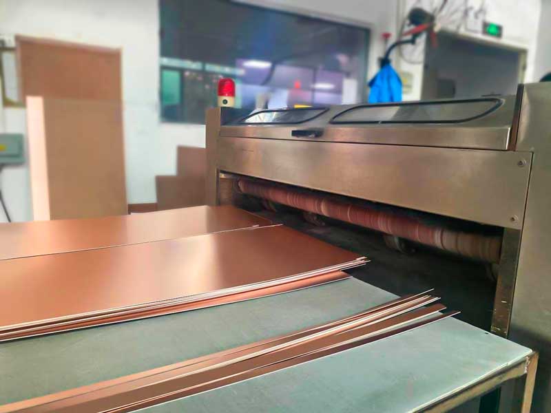
Producing a circuit on ceramic requires a copper-clad ceramic substrate first, and there are two routes to it. The lamination route presses an oxidised copper foil against the alumina substrate: the ceramic surface is first activated or roughened, for example by laser or plasma treatment, and then a stack of copper foil, a heat-resistant adhesive layer, the ceramic, a second adhesive layer, and a second foil is fired at around 1,020 to 1,060 degrees Celsius to form a double-sided copper-clad ceramic laminate.
The plating route treats the substrate with plasma and then deposits titanium, nickel, and copper films by sputtering before electroplating copper to the required thickness. That produces the same substrate by a different means. From that point, single-sided and double-sided ceramic boards are made with conventional board processes, which is why a ceramic substrate is best understood as a relative of the ordinary PCB rather than a separate technology.
Multilayer Ceramic Boards
Multilayer ceramic construction follows one of two paths. The first builds the layers sequentially: an insulating alumina layer is coated, fired, patterned, and fired again, repeated until the stack is complete. The second uses tape casting directly, as described earlier: green tape is formed, drilled, filled with conductive paste, printed with the conductor pattern, cut, stacked, and bonded under isostatic pressure and high temperature in a single co-firing step.
The second route is the one that produces multilayer ceramic substrates and ceramic chip capacitors at volume, because the layers are processed in parallel before being bonded together. The supplier-side view of how a stack is specified and verified is discussed in multilayer PCB prototype requirements, and the general principles of layer ordering in layer stackup from one to eight layers.
Direct Bonded Copper and Ceramic Reliability
Most power ceramic substrates use direct bonded copper, in which a copper sheet is bonded to the alumina surface at high temperature so that the copper-oxygen eutectic forms the joint. The result carries heavy current, spreads heat laterally, and survives thermal cycling that would fatigue a soldered joint, which is why the construction appears in inverter and motor-drive modules. It is the same heat-removal problem that a metal core board solves by another route, and the two approaches are compared in metal core PCB thermal management.
Reliability is where the ceramic route earns its cost. A module that cycles between ambient and a high junction temperature thousands of times will eventually fatigue a solder joint on an organic substrate, whereas the ceramic body itself does not creep or soften. The trade is that ceramic is brittle and its coefficient of thermal expansion is lower than that of copper, so the design has to keep the bonded copper area balanced and avoid concentrating stress at the edge of a bonded region.
FAQ
Why does a ceramic part need machining after firing? Because sintering distorts the green body. Polishing restores flatness and finish, and the expected distortion has to be anticipated in the tooling as well.
What is the difference between hot pressing and hot isostatic pressing? Hot pressing applies pressure along one axis and gives good flatness. Hot isostatic pressing uses high-pressure gas so the whole part sees uniform conditions, which costs more and is reserved for high-value applications.
How is copper attached to a ceramic substrate? Either by laminating an oxidised copper foil with a heat-resistant adhesive and firing it, or by sputtering titanium, nickel, and copper and then electroplating to the final thickness.
Why fire the layers together rather than one at a time? Co-firing a stacked green tape processes all the layers simultaneously, which is faster and more uniform, and it is how multilayer ceramic substrates are produced in volume.