Ultrasound Probe PCB Design: Channels, Materials and Stackup
An ultrasound probe is a dense analogue front end wrapped in a hand held package. Its printed circuit board carries the transmit pulses, the returning echoes, the beamforming connections and the control signals, all inside a body small enough to press against a patient. That combination of high channel count, microvolt signal levels and tight mechanical space makes the ultrasound probe PCB one of the more demanding mixed signal boards in medical electronics. This guide covers the decisions that decide whether the design works: stackup and channel routing, material selection, noise and crosstalk control, thermal limits, transducer interconnect and the test plan.
What an Ultrasound Probe PCB Has to Do
The board sits between the piezoelectric transducer array and the system cable or the on-probe electronics. It distributes high voltage transmit pulses to each element, receives microvolt level echoes back from the same elements, and often hosts preamplifiers, multiplexers, time gain compensation and part of the beamforming chain. In a hand held device, analogue to digital conversion and digital signal processing may happen on the probe itself, which puts the whole receive path inside the handle.
That mix of a high voltage transmit path and a very low level receive path on the same small substrate is the central design difficulty. The two paths must be separated physically, referenced carefully and sequenced so that transmit switching does not corrupt the receive channel that is about to listen. Everything else in the layout follows from how well that separation is planned before routing begins.
Channel Count and the HDI Stackup
Probe arrays run from a few tens of elements to several thousand, and each element needs a signal connection, a ground return and often a control line. A high density interconnect stackup with fine lines, small microvias and thin dielectrics is the usual answer, sometimes built as any layer HDI so that a via can be placed wherever the escape routing needs one rather than only on a drilled core.
Multi-channel routing also drives the layer count and the layer order. Placing analogue receive traces next to a quiet ground plane, with transmit and digital layers separated by reference planes, gives the layout team room to keep sensitive nets short. Rigid flex construction is common, because the probe face, the handle and the cable exit sit at different angles and a single flat board cannot follow the mechanical envelope.
Materials for Low Loss and Phase Stability
Receive signals are weak and the path to the system is long, so every decibel of insertion loss counts. A low loss material keeps the received echo and the transmit pulse intact over the length of the board, and a stable dielectric constant keeps the delay through each channel consistent from probe to probe and across the operating temperature range.
Where the probe works at higher frequencies, or where delay matching between channels affects the beam, the dielectric constant and its temperature coefficient become specification items rather than background details. Material choice also reaches into the acoustic design, because the layers behind the transducer influence how each element radiates and how the backing absorbs energy that would otherwise ring.
Noise, Crosstalk and Grounding
The signal-to-noise ratio of the receive channel sets the achievable image quality, and protecting it means keeping the return path continuous under every analogue trace, placing the preamplifier as close to the element as the mechanics allow, and preventing digital switching currents from sharing the same ground copper as the receive front end.
Crosstalk is the other hard limit. Adjacent channels couple through the dielectric and through shared return paths, and in a phased array that coupling appears as amplitude and phase error across the aperture. Stitching ground between channels, maintaining spacing between traces and using differential routing on critical nets all reduce it. Our guidance on mixed signal PCB design sets out the separation rules in more detail.
Thermal Limits in a Handheld Probe
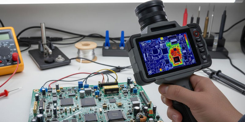
A probe resting against skin has a surface temperature limit set by patient safety standards, and the transmit path is the dominant heat source. The duty cycle is short but the peak power delivered to the transducer is high, so the board has to move heat into the handle and away from the face rather than simply dissipating it locally.
Copper area on the transmit and regulator sections, thermal vias into internal planes and a deliberate conductive path into the metal chassis all help. Where the electronics are integrated into the probe, package choice and component placement decide whether the limit can be met at all, and a thermal simulation before layout freeze is far cheaper than discovering the problem during a compliance test.
Interconnect to the Transducer
Attaching the transducer array to the board is a mechanical and electrical problem at the same time. Fine pitch flex tails, anisotropic conductive film, wire bonding and solder bumping are all used in production, and each sets its own requirements for pad geometry, surface planarity, cleanliness and the thermal budget the assembly can tolerate.
The board also has to survive assembly and handling. Reinforcement, stiffeners and structural adhesives control how the flexible tail behaves when the probe is bent, and the attachment must hold through thermal cycling and repeated disinfection. Our notes on FPC stiffener comparison and PCB cable assembly cover the practical options.
Testing and Manufacture
A probe board is normally tested at three levels: bare board continuity and impedance on coupons, assembled board in circuit test with the front end powered, and functional testing against a known acoustic target. Because the channels must match one another, gain and delay are measured per channel and trimmed where the design allows, and the results are recorded for traceability.
Manufacture also has to be clean. Contamination on a transducer interface or under a bonded flex tail creates a field failure that no electrical test will catch, so solder mask, via fill and cleaning processes are specified for the assembly environment rather than for the lowest possible cost. See any layer HDI PCB and high density interconnect PCB for the fabrication side.
Design Review Checklist for a Probe Board
Before the layout is released, a short review catches most of the failures that would otherwise appear at functional test. Confirm that every analogue receive net has an unbroken reference plane beneath it, that the transmit and receive sections are physically separated with their own return currents, and that the preamplifier sits within the distance the source impedance can tolerate. Check the channel to channel length skew against the delay matching the beamformer assumes, and confirm that the flex tail transition does not create an impedance discontinuity that the tuning network has to absorb.
Then look at the mechanical and thermal interfaces together. Verify that the stiffener positions match the bends the probe will actually see, that the transducer bond pads are reachable with the assembly process chosen, and that the thermal path out of the transmit driver has been modelled rather than assumed. Finally, confirm that the test plan covers per channel gain and delay measurement, because an array that passes continuity testing can still fail acoustically if two channels are mismatched. A checklist of this kind costs an hour and prevents most of the expensive iterations on this type of board.
FAQ
What type of PCB does an ultrasound probe use? Most are multilayer high density interconnect boards, frequently in rigid flex construction, because the probe face, handle and cable exit need different orientations and the channel count demands fine lines and small vias.
Which material is best for the receive path? A low loss laminate with a stable dielectric constant suits high frequency probes, while conventional FR4 remains adequate for lower frequency, shorter channels where the loss budget allows it and the cost saving matters.
Why does crosstalk matter so much in an array? Because neighbouring elements are compared to form a beam. Signal coupled between channels shifts amplitude and phase across the aperture, and the resulting degradation cannot be corrected after the fact by software alone.
Related reading: ceramic substrate materials.