PCB Reverse Engineering: Tools, Steps and Legal Limits
Reverse engineering a board is a legitimate engineering task with a bad reputation, mostly because the same techniques serve both maintenance and copying. In practice it is how a discontinued controller gets supported, how a legacy product is documented after the original files are lost, and how a failure in an obsolete assembly is finally understood.
What Reverse Engineering Is Used For
The common cases are practical rather than competitive. A product whose design files were never archived needs documentation before it can be repaired. A board that must remain in service for another decade needs a second source for obsolete parts. A field failure in an assembly with no schematic needs to be traced to a specific net.
Understanding the intent shapes the method. Repair work needs connectivity and component values. Re-manufacture needs dimensions and layer information. Failure analysis needs the same connectivity but at a finer level of detail, including which nets share a reference plane.
Step 1: Component Identification
Documentation starts with the physical board. Record the layer count, the board thickness, the surface finish and the outline dimensions, then photograph both sides at high resolution so that silkscreen markings, part numbers and date codes remain readable.
Identify each component and record its designator, value, package and tolerance. Where a marking is ambiguous, measure the part. A capacitor with no visible value can be measured in circuit for capacitance, and a resistor can be read directly once one end is lifted.
Step 2: Net Tracing and Continuity Mapping
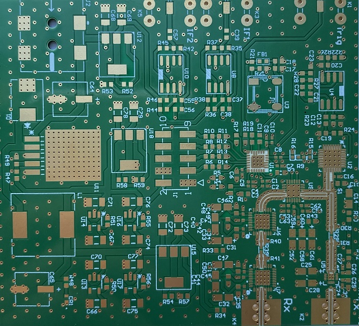
Continuity testing builds the netlist. Working from the connector inward is usually the most efficient order, because the connector pins give the circuit an obvious boundary and establish which supply rails and grounds are present. A multimeter with a continuity beeper and fine probes is enough for a two-layer board.
For multilayer boards the work becomes harder because inner layers are invisible. Probing accessible vias and pads, watching where the plane layers connect, and removing selected components to expose hidden traces all help, but each removal risks damage and must be done with care.
Recording the results as you go is essential. A netlist built from memory will contain errors that only appear when the schematic is checked against the board a second time.
X-Ray Inspection of Multilayer Boards
X-ray inspection answers the question that continuity testing cannot: how the inner layers are connected. A two-dimensional X-ray shows the copper pattern of each layer superimposed, and with the board tilted or rotated, buried vias and inner traces can be traced without destroying the sample.
Computed tomography goes further and reconstructs the layers, which is the closest thing to seeing the artwork. It is slower and more expensive, so it is normally reserved for a board that must be documented exactly.
Step 3: Schematic Capture and BOM
With the netlist complete, the schematic is captured in a design tool. Each part is given a value and a symbol, and nets are named meaningfully rather than left as generated identifiers. This is where errors surface: an inferred connection that contradicts the continuity data usually means a probe slipped or a trace was misidentified.
The bill of materials is built alongside the schematic. It lists every part with a manufacturer part number where known, and with a functional description where the original is obsolete. Identifying acceptable substitutes is part of the deliverable, not an afterthought.
Step 4: Recreating the Layout
Rebuilding the layout means matching the mechanical envelope first: outline, mounting holes, connector positions and keep-out areas. The routed geometry is then recreated, and here the goal matters again. An exact copy preserves behaviour but also preserves every original compromise, while a redesign can improve return paths, thermal relief and test access.
Where the board is being re-manufactured, staying close to the original is usually correct. Where it is being modernised, the schematic becomes the input and the layout is treated as a new design.
Tooling and Software
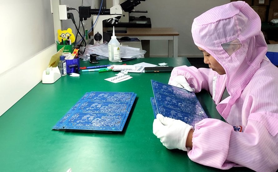
The toolset is modest. A stereo microscope and a high-resolution camera document the board, a multimeter handles continuity, and X-ray covers the inner layers. A precision caliper measures features that must be replicated, and hot air or an IR station removes components without lifting pads.
On the software side, an open source schematic and layout package is sufficient for the schematic capture and the new layout. Gerber viewers help compare the reverse engineered artwork against the original copper pattern by overlaying the two images.
Documentation Practices That Save Rework
Photograph every step, including the position of each part before it is removed. Keep a running netlist rather than a set of notes, and verify each measurement twice. Where a value is inferred rather than measured, mark it as inferred so that a later reviewer knows which numbers to distrust.
Two habits pay off repeatedly. First, cross-check the finished schematic against the board by re-testing a sample of nets, chosen to cover both obvious and obscure connections. Second, record the board revision and serial number, because two units of the same product may not be identical.
Legal and Ethical Boundaries
Reverse engineering is lawful in many contexts and unlawful in others. Repairing equipment you own, documenting a product you manufacture, and studying interoperability are generally accepted. Reproducing a protected design for commercial sale is not, and patents, copyright and trade dress all apply.
Compliance obligations continue alongside intellectual property law. Re-manufactured assemblies are expected to meet the same design and fabrication practice as any new build, and where the product is documented for a redesign, the quality characteristics of the original are worth recording before the layout is changed. A short review of PCB construction fundamentals helps a team decide which properties must be preserved exactly.
Choosing Between Repair, Documentation and Redesign
PCB reverse engineering is a spectrum rather than a single service, and the right depth depends on the objective. Supporting a single unit in service needs connectivity and component values. Re-manufacturing a product needs a complete fabrication package. Modernising a platform needs only the schematic and the functional requirements, because the layout will be rebuilt from scratch anyway.
Deciding which one applies before starting saves a great deal of effort. A team that documents every trace for a redesign spends weeks producing data it never uses, while a team that captures only a schematic for a re-manufacture discovers later that the mechanical envelope was never measured.
Write the objective down and let it drive the level of detail. It also determines the tooling: continuity testing and photographs for repair work, X-ray and cross sections for exact reproduction, and simulation for a modernised design.
FAQ
Can a board be reverse engineered without removing components? Often yes, at least to the netlist level. Continuity testing and X-ray cover most of the work, and selective removal is only needed where a hidden trace or a questionable component value blocks progress.
How accurate is an X-ray reconstruction? Accurate enough to identify layer connections and trace routing, particularly with computed tomography. It is less reliable for fine measurement of conductor width, which is better confirmed with a cross section.
Is reverse engineering the same as copying? No. The technique produces documentation, and what is done with that documentation is a separate decision governed by law and by contract. Where the goal is repair or modernisation, the work is usually unremarkable; where the goal is copying a protected design, it is not, and see multilayer prototype requirements for how a compliant rebuild is normally specified.