PCB Copper Pour: Grounding, Vias and Thermal Relief
A copper pour is the area of metal left on a signal layer after the traces have been routed. It is often added at the end of a layout as a habit, but it is an electrical structure with a defined purpose, and a pour that is added without a plan can make a circuit worse rather than better.
The pour can act as a reference plane, as a thermal spreader, as a shield or simply as a way to balance copper for etching and lamination. Which of those roles it is playing decides how it should be connected and how it should be divided.
What a Copper Pour Is For
The most common purpose is to provide a return path beside a signal. A trace with a plane underneath it has a defined impedance and a small loop area, and the return current follows the trace rather than finding its own way around the board.
The second purpose is thermal. Copper beside a power device spreads heat over an area larger than the component, which reduces the local temperature rise and helps the heat reach a thermal via or an edge.
Solid Versus Hatched Pour
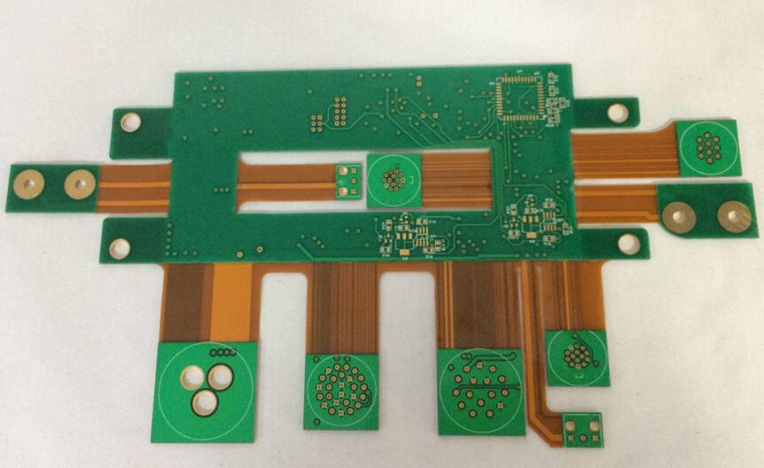
A solid pour gives the lowest impedance and the best thermal performance, and it is the normal choice on a rigid board. Its disadvantage appears on a flexible circuit or on a thick copper layer, where a large continuous area can delaminate or crack under bending.
A hatched pour is used in those cases. The hatch keeps the copper connected while allowing the material to flex, and it also reduces the mass of copper that has to be etched away. The hatch spacing is chosen to be small compared with the shortest wavelength of interest, so that the structure still behaves as a plane.
Stitching Vias and Return Paths
A pour on a signal layer is only a reference if it is connected to the ground system. Stitching vias tie the pour to the ground plane, usually on a grid around the board edge and beside every trace that crosses a boundary.
The spacing follows the highest frequency present. As a rule, the vias are placed at intervals well below a quarter wavelength at the highest frequency of interest, and closer where a trace changes layer or where the pour forms a narrow neck between two regions.
Thermal Relief on Pads
A pad that connects to a large pour through solid copper is difficult to solder, because the copper conducts heat away from the joint faster than the iron or the reflow process can supply it. A thermal relief replaces the solid connection with a set of narrow spokes, which raises the thermal resistance during soldering while keeping the electrical connection.
The number and width of the spokes are a compromise. Fewer spokes make soldering easier and increase the thermal resistance, which is acceptable on a signal pad and unacceptable on a ground pad that has to carry current or heat.
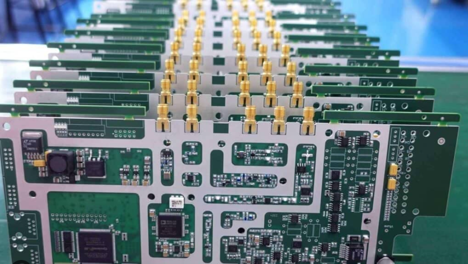
Islanding and Isolated Copper
A pour that is not connected to anything is an antenna. Small islands of copper left inside a routed area can float at an undefined potential, couple to nearby traces and radiate, and they are almost always a defect rather than a feature.
Design tools usually offer a setting to remove isolated islands below a defined area. That setting should be used, and the remaining pour should be checked for narrow necks that connect a useful region to a remote one, because a long thin connection behaves as an inductor rather than as a plane.
Pour on Power Nets
A pour is not only for ground. On a power net, a pour reduces the DC drop and provides local charge storage in combination with the decoupling capacitors. It also complicates the layout, because two power pours on the same layer have to be separated by a gap that satisfies the voltage clearance.
Where a power pour is used, its connection to the load is as important as its area. A wide neck between the pour and the pins of the device is what makes the resistance low, and a pour that reaches a component through a single narrow trace has gained nothing.
Effect on Impedance and EMI
A pour beside a trace changes the impedance, because the field distribution is no longer that of an isolated line. On a coplanar structure the pour is part of the transmission line, and its spacing to the trace is a design parameter rather than a filler.
From an emissions point of view, a grounded pour reduces the loop area of every trace it neighbours, which lowers the radiated field. A floating pour does the opposite, which is why the connection of the pour matters more than its presence.
Design Rules and Checklist
Decide the purpose of the pour before adding it, connect it to ground with vias on a spacing that suits the highest frequency in the design, use thermal relief on pads that have to be soldered, remove isolated islands and keep narrow necks out of any region that is meant to behave as a plane.
gopcb builds boards with copper balancing, controlled impedance and the pour connectivity that high speed designs require, and can review a layout for float islands and return path discontinuities before the panel is released.
Pour on Mixed Signal and RF Boards
The pour is where a mixed signal design either succeeds or fails. An analog section wants a quiet reference and a pour that is connected at one point to the digital ground, while a digital section wants a low impedance return path for fast edges. If a single pour covers both, the return current from a digital trace can flow through the copper beneath an analog input and couple switching noise into it.
The usual solution is a partition rather than two separate grounds. The pour is divided along a defined line, the two regions are joined at one point beneath the converter, and no trace crosses the divide without a stitching capacitor or a return via beside it. The rule is not that grounds must be separate, but that every return current must have a defined path home.
Pour and Copper Balance for Fabrication
Pours also serve the fabricator. A layer with a large empty area etches differently from one with a dense pattern, and uneven copper distribution causes the laminate to press unevenly, which shifts the layer registration and changes the dielectric thickness. Adding a balanced pour, or thieving bars on the panel, is a way to make the process more predictable.
The pour is therefore part of the fabrication drawing rather than only a layout convenience. Where copper is added for balance rather than for electrical function, it should be identified as such, so that a later revision does not remove it as redundant and introduce a thickness variation that affects every controlled impedance trace on the board.
FAQ
Should every layer have a copper pour? No. A pour helps where a return path, thermal spreading or copper balance is needed, and it becomes a liability where it creates floating islands or where it interferes with a controlled impedance structure.
Why does a pad on a plane solder poorly? Because the plane conducts heat away from the joint. A thermal relief reduces the heat loss during soldering while keeping the electrical connection.
Does a copper pour reduce electromagnetic emission? A grounded pour reduces the loop area of adjacent traces and therefore lowers the emitted field. An unconnected pour can make the emission worse.
Related reading: power plane design, ground current and harmonic distortion, mixed signal PCB design guidelines, and trace width and current calculation.