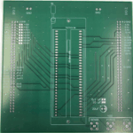
Difficult Board Prototypes: Layout and System Test
Some boards are difficult for reasons that have nothing to do with the circuit diagram. Fine pitch devices, controlled impedance, mixed analogue and digital sections and tight mechanical constraints all push the design outside what a generic layout can support. Building one successfully depends on treating the layout and the test programme as a single exercise.
What Makes a Board Difficult
Difficulty usually comes from one of four sources: the frequency of the signals, the density of the components, the precision of the mechanical requirement or the sensitivity of the analogue front end. A board that combines two of them is where most prototype failures occur.
Recognising the difficulty early changes the plan. The layer count, the stackup, the simulation effort and the test access all have to be decided together, rather than being adjusted as the design progresses.

Layout Principles for High Speed
Components should be arranged evenly and compactly, with the connections between them as short as the routing allows. A tidy arrangement is not an aesthetic preference at high frequency: every extra millimetre of trace is inductance that changes the edge and the delay.
The routing has to follow the reference planes rather than the shortest path on the screen. A trace that crosses a plane split loses its return path and radiates, so continuity of the reference is a constraint on every net that carries a fast edge.

Separating Analogue and Digital
The analogue section is sensitive and the digital section is noisy, and the layout has to keep them apart. That begins with placement, continues with the partitioning of the planes and ends with the return currents, as the general guidance for mixed-signal boards describes.
Where separation is impossible, a defined boundary and a single crossing point confine the coupling to a place where it can be controlled. Scattered crossings of the boundary make the noise path unpredictable and the diagnosis much harder.
Clock Placement
The clock is the single most important net on a high speed board. It should be placed where it can reach its loads by the shortest route, kept away from connectors and interface cables, and referenced to a ground plane that is continuous beneath it.
Where a clock must be distributed, the routing should be treated as a transmission line rather than a wire, and the jitter budget shared with the devices it drives, as the design of an ADC clock network illustrates. A clock that reaches its load with a distorted edge will degrade the performance of everything downstream.
Simulation Before and After Routing
Pre-layout analysis fixes the topology: which nets need termination, how long the critical paths may be and what impedance each class requires. Its purpose is to set constraints that the layout can then honour.
Post-layout analysis verifies that the routing met them. Where a critical delay matters, the routes are matched to a budget, using length matching for the difference, and the extraction confirms the result rather than the intention.
Prototype Build and Bring-Up
The first article should be built with the same process the production board will use, because the assembly method affects the result. Hand assembled samples tell you about the circuit, not about the manufacturability of the design.
Bring-up follows a fixed order: verify the supplies and their sequencing before powering the active devices, confirm the clock is present and clean, then check the interfaces one at a time. Applying power to an unverified supply is the quickest way to destroy the parts the prototype was built to evaluate.
System Test and Margin
Functional test at nominal conditions proves very little on a difficult board. The requirement is margin: supply variation, temperature extremes, loading changes and timing shifts, each measured against the specification rather than against a pass or fail threshold.
Design margin is what separates a prototype that works on the bench from a product that works in the field. Where the margin is thin, the design needs attention before release rather than a note in the test report.
EMC Measurement
Compliance is demonstrated by measurement, not by design intent. Radiated and conducted emissions are measured across the relevant frequency range, and the results are compared against the limit with the same attention to margin that the functional tests received.
Where a problem is found, the source is usually the switching supply or a clock, and the remedy is at the source rather than the antenna. The rules for supply layout address most of the cases that appear during pre-compliance testing.
Fixtures and Test Access
Difficult boards usually need test points that a generic design would not require: access to the clock, to the supplies and to the interfaces that are hard to probe once the product is closed.
The points should be designed into the layout with adequate size and spacing, and a fixture that holds the board reliably is part of the prototype budget rather than an afterthought. A board that cannot be measured consistently will be debugged by intuition, which is slower and less reliable.
Iteration Strategy
A difficult board is rarely finished in one pass, so the first prototype is a measurement instrument as much as a product. It should be built to answer specific questions, and the questions should be written down before the layout is released.
Revisions should then change one class of thing at a time. Changing the stackup, the placement and the termination network together guarantees that whatever fixed the problem is unknown, and the second prototype teaches nothing except that the third is needed.
Layer Count and Stackup
The stackup follows from the routing requirement rather than from habit. Counting the signal layers needed to escape the dense devices, then adding the planes needed to reference them, gives the minimum practical layer count.
Symmetry and material choice complete the decision. A symmetric stackup keeps the board flat through the multiple reflow cycles that a populated prototype will see, and the dielectric properties determine the impedance of every controlled trace.
Working With the Fabricator and Assembly House
Difficult boards should be quoted and reviewed before the artwork is finalised. Capability questions about minimum features, filled vias, impedance tolerance and panel construction are answered more cheaply at that stage than after the order is placed.
The assembly house should be involved for the same reason. Stencil design, thermal profile and inspection coverage all depend on the package mix, and their requirements feed back into the pad design and the placement rather than being applied afterwards.
Documenting the Prototype
Record what was built and why: the stackup, the design rules in force, the simulation results and the assumptions behind them. A prototype without its documentation is a board with an unknown specification, and its results cannot be trusted or repeated.
The record should also include what the prototype disproved. A negative result is information, and it prevents the next revision from re-testing an idea that was already eliminated at some cost.
FAQ
When should a design be treated as difficult? When any single requirement exceeds the routine process: fine pitch devices, controlled impedance, frequencies above a few hundred megahertz or a genuinely sensitive analogue front end.
Is simulation necessary on a difficult board? A basic stackup calculation and a routing review are always worthwhile. Full analysis earns its cost where a failed prototype would delay the project by weeks.
What is the most common cause of a failed bring-up? An unverified supply or a missing clock. Checking those two before applying full power resolves a large share of first article faults without any risk to the components.