Driver PCB Cost: What a Driver Board Really Costs
A driver board sits between a control signal and a power stage, and its cost is set by the power it handles rather than by the logic it contains. Current, switching frequency and isolation distance each push the specification in a different direction, and the board you end up with is the compromise. This guide explains how a driver PCB cost is built in 2025.
What a Driver Board Has to Do
The protection function is often the largest component count on the board. Desaturation detection, overcurrent sensing, a clamp network and an undervoltage lockout each require components and layout attention, and they scale with the number of power devices being driven rather than with the load power itself.
A driver board converts a low-level control signal into the current and the timing needed by a power device. It provides a gate driver or a base drive stage, it sets the switching speed, it protects the power device from overcurrent and overvoltage, and it often provides the isolation barrier between the control side and the load side.
Each of those functions has a cost consequence. The drive stage sets the component count, the protection sets the sensing and the clamping, and the isolation sets the board area because a barrier cannot be routed across. The logic, by contrast, is almost free.
Current, Copper Weight and Board Area
Current is the first cost driver. A driver that handles a few amps can use 1 oz copper and modest conductors, while one that handles tens of amps needs 2 oz or heavier copper and conductors sized by trace width and current with a temperature rise allowance. Heavy copper is priced across the whole panel rather than only on the high-current nets.
Board area follows the current in a way that surprises designers. Wider conductors, larger terminals and greater clearance all consume area, and area is charged twice: once as material and once as process time per panel. A high-current driver is therefore bigger and more expensive per function than a signal board.
Gate Drive and Switching Losses
The gate drive stage determines how fast the power device switches, and switching speed determines the loss balance between conduction and switching. A faster gate loop needs a lower-impedance driver, a tighter layout and often a separate gate resistor per device, all of which add components rather than remove them.
Loop inductance is the hidden parameter. A gate loop with a large enclosed area produces ringing, which forces a slower switching speed and increases loss, and the usual remedy is a layout change rather than a component change. Applying converter layout and routing principles to the gate and power loops is what keeps the design predictable.
Thermal Path and Heatsinking
Thermal vias are the cheapest tool available. A cluster of small vias under a power device lowers its junction temperature significantly, and the cost is a drilling operation rather than a material change. They should be sized and spaced by the thermal calculation rather than by habit.
The thermal path decides the package, the copper area and often the board construction. A driver dissipating a few watts can use a copper pour and thermal vias into an internal plane, while a higher-power stage needs a metal-backed substrate or a heatsink bolted through the board.
Each step in that progression adds cost and a process. An aluminum substrate removes a mechanical part but limits the routing to one side, while a heavy copper inner plane adds material and lamination time. The decision should come from a measured junction temperature rather than from a general rule of thumb.

Isolation and Creepage
The isolating component itself is priced by the working voltage and the certification required, not by its package size. A device rated for the barrier and supported by the appropriate approval documentation is worth more than a cheaper alternative that would need additional evidence at qualification.
When the driver bridges a control side and a mains or high-voltage load, an isolation barrier is mandatory. Creepage and clearance have minimum values that depend on the working voltage, the pollution degree and the material group, and the barrier itself consumes board area because no copper may cross it except through the isolating component.
Isolation also constrains the layer assignment. A barrier that is adequate on the surface may be defeated by an inner layer carrying a signal across it, so the routing of the whole board has to respect the barrier rather than only the immediate area around the isolating device.
Layer Count and Layout
The return path deserves as much attention as the forward path. Current leaves the supply, passes through the power device and the load, and returns to the supply, and the area enclosed by that loop radiates. Keeping the return directly beneath the forward path on an adjacent layer is the standard remedy.
Most driver boards run on two to four layers. Two layers are adequate when the current is modest and the isolation is simple, while four layers become worthwhile when a continuous ground plane is needed to control the gate loop and to carry the return current of the power stage.
Above four layers the reason is usually thermal or mechanical rather than electrical. A board with several power devices and a heavy copper requirement may need additional layers to distribute current and heat, and at that point the cost increase is driven by the material rather than by the routing.
Prototype, Assembly and Test Cost
Selective soldering is the assembly step that most often surprises a budget. It needs a fixture and a programme, and it runs at a lower rate than reflow. Reducing the through-hole content, where the thermal requirement allows it, removes that step entirely.
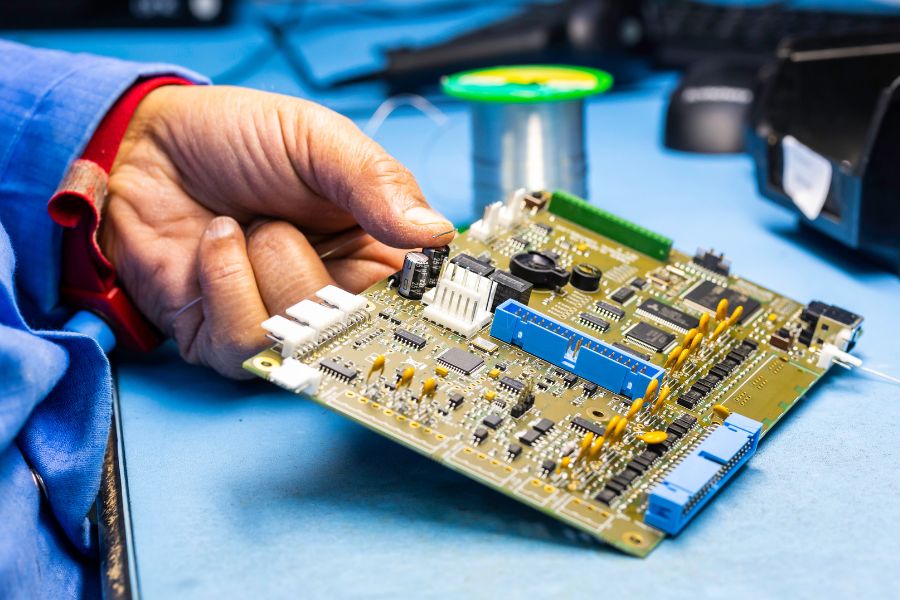
The pcb prototype cost of a driver board is dominated by assembly and test rather than by fabrication. Power devices are often through-hole or press-fit parts, which require selective soldering and a fixture, and a functional test at full load needs a load bank and a thermal measurement rather than a simple continuity check.
Test coverage matters because a marginal gate drive or a poor thermal joint does not fail on the bench. A functional test that runs the board at load and measures the device temperature catches both, and it costs seconds per unit once the fixture exists.
Reducing Cost Without Losing Margin
Stay with the lightest copper that satisfies the current and the temperature rise, keep the isolation barrier as compact as the standard allows without reducing the distance, and use a standard substrate unless a measurement shows that a metal core is required. Each of those decisions removes a process step.
Applying manufacturable design guidelines then keeps the rest of the board on a routine flow. What should not be reduced is the gate loop area, the thermal path under the power devices or the isolation distance, because those three items decide whether the board survives its own switching.
FAQ
Why does a driver board cost more than a similar-sized logic board? Copper weight, thermal construction, isolation area and assembly complexity. A driver board carries current, spreads heat and often has to bridge a safety barrier, and each of those adds material or process rather than logic.
Do I need an aluminum substrate for a driver board? Only when the thermal measurement requires it. Copper pours with thermal vias handle a surprising amount of dissipation, and they keep the board on a standard FR-4 process with routing available on both sides.
How is a driver board tested? At load, with the power device running and its temperature measured. A continuity or logic test does not exercise the gate loop or the thermal joint, which are the two most common sources of a failure in the field.