Eight Layer Board Fabrication: Process Step by Step
An eight layer board is built from the same materials as a two-sided board and passes through many of the same operations, but the sequence is longer and the tolerances are tighter. The additional steps are what allow the layer count, and they are also what make the process sensitive to decisions taken during the design. Understanding the sequence makes it easier to see why certain design rules exist.
What Makes a Multilayer Board Different
A double-sided board has one dielectric layer with copper on both faces. A multilayer board stacks several conducting layers with dielectric between them, joining the layers electrically with plated holes that pass through the stack. The dielectric between inner layers can be made very thin, which is what allows the close spacing between a trace and its reference plane.
The construction is what provides the electrical benefit, and it also creates the manufacturing complexity. Each inner layer has to be imaged and etched before the stack exists, and the layers then have to be joined in a way that keeps them aligned to each other within a tolerance measured in tens of micrometres.
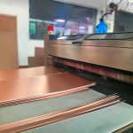
<img src="https://www.gopcba.com/wp-content/uploads/2024/09/tupian3.png" alt="eight layer board during lamination and drilling” />
Inner Layer Processing
The process begins with the inner layers of the eight layer board. Copper-clad laminate is cleaned, a photoresist is applied, the artwork is exposed and developed, and the exposed copper is etched away. The result is a core with the required pattern of traces, pads and planes on both faces.
Each core is then inspected and the copper surface is treated so that it will bond to the resin during lamination. Surface treatment matters more than it appears, because a bond that is weak at this stage will delaminate later, and delamination inside a finished board is invisible until it causes a failure. The artwork itself should already have accounted for the way the panel moves during the remaining processes, which is described in this article on dimensional stability.
Lamination and Registration
The cores are then stacked with prepreg between them, copper foil on the outside, and pressed under heat and pressure. The resin in the prepreg flows, fills the gaps around the copper features and cures, bonding the layers into a single panel.
Registration is the critical parameter. The layers must remain aligned with each other while the resin flows, and the target tolerance is small enough that the material behaviour matters. Registration is checked with targets at the panel corners and sometimes in the interior, and the measured values determine whether the clearances the designer specified have been achieved. A design whose tightest features sit at the panel edge is exposed to the least favourable registration, which is one reason pad sizes have to be larger than the theoretical minimum. The relationship between these clearances and the hole geometry is described in this discussion of via to trace clearance.

Drilling and Plating
After lamination the panel is drilled. The drilling programme produces every hole in the design, from the smallest via to the largest mounting hole, and the accuracy of the hole position relative to the copper is what determines the annular ring around each hole.
Plating then deposits copper into every hole and across the surface. The electrolyte must circulate through the holes, and the plating thickness at the middle of a hole is always less than at its ends. Where a design requires a via whose depth is large relative to its diameter, that difference becomes significant, and the structures used to address it are described in this article on blind via and buried via stack selection. After plating, the outer layers are imaged and etched, the solder mask and silkscreen are applied, the surface finish is deposited and the profile is routed.
Where the Design Influences the Result
Design decisions influence the fabrication sequence at three points. The layer arrangement determines the dielectric heights and therefore the impedance, and it also determines how much copper exists on each layer and therefore how much the panel will move during lamination. The via sizes determine whether the drilling and plating operations run inside their process windows. The feature density determines whether the etching is uniform across the panel.
All three are fixed before the design is released, and changing any of them afterwards invalidates the work that depended on it. That is why the stackup should be agreed with the fabricator early, and why the prototype requirements reviewed before volume production include the stack rather than only the artwork; the checks involved are set out in this discussion of multilayer prototype requirements.
Comparing Constructions
An eight layer board is usually chosen when the routing density or the reference requirements exceed what six layers can provide. The additional layers allow each signal layer to have a close reference and allow the power distribution network to be separated from the signal references. The cost of the additional layers is real, and it should be justified by a requirement rather than by a preference.
The arrangement of the layers matters as much as the count, and the principles that determine a good arrangement are described in this article on layer stackup design.
Registration and Layer Count Discipline
Registration is the thread that runs through the whole eight layer board sequence. Each inner layer carries targets that must survive etching, oxide treatment and the press cycle, and the accumulated tolerance decides whether the finished stack can still be drilled without shorting to an inner plane. A fabricator that measures scaling on every layer and compensates the artwork before imaging will hold the stack far more tightly than one that trusts the nominal drawing. When the layer count rises, so does the number of interfaces, and the tolerance budget has to be split across all of them rather than spent entirely on the drill.
Layer count discipline matters just as much at the design stage. Every added pair of layers costs imaging, etching, lamination and drilling time, so the question is not whether more layers are technically possible but whether the routing genuinely needs them. Reference planes, controlled impedance traces and high speed differential pairs are the usual reasons to step up, and each of those requirements should be checked against a cheaper alternative before the stack is frozen. A design that commits to eight layers for convenience rather than necessity pays the penalty on every unit it builds, which is a price that never goes away.
FAQ
Why does an eight layer board cost more than a four layer board? Because it contains more inner layers to image and etch, more lamination interfaces to bond, and a longer process sequence with more opportunities for a registration error. The cost is driven by the number of operations rather than by the area of the board.
What is registration and why does it matter? Registration is how accurately the copper features on one layer line up with those on the others after lamination. It determines whether the clearances the designer specified actually exist in the finished board, and it becomes harder to hold as the layer count and panel size increase.
Can the stackup be changed after the layout is complete? Not without repeating the design work that depends on it. The dielectric heights set the impedance of every controlled trace, and the copper distribution affects how the panel moves during lamination. A stack change invalidates the impedance calculations and the clearance assumptions.