What Is an ENIG PCB?
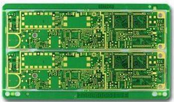
A printed circuit board is the foundation of many electronic products, providing electrical connections, component mounting, and signal transmission. Among the various surface finishing technologies available today, ENIG PCB has become a popular choice for applications requiring a smooth surface, reliable solderability, corrosion resistance, and consistent electrical performance.
ENIG stands for Electroless Nickel Immersion Gold. The process deposits a layer of electroless nickel onto exposed copper and then applies a thin layer of immersion gold over the nickel surface.
Unlike electroplated finishes, electroless nickel deposition does not require an external electrical current. Instead, a controlled chemical reaction forms a relatively uniform nickel layer, followed by the immersion gold layer.
This nickel-gold structure provides a combination of mechanical protection, surface stability, solderability, and corrosion resistance, making ENIG suitable for a wide range of advanced electronic applications.
For projects requiring different board structures and surface finishing options, GOPCBA provides comprehensive PCB Manufacturing Services for prototype and production requirements.
How Does ENIG Surface Finish Work?
The performance of an ENIG Surface Finish depends on the controlled formation of two metallic layers: electroless nickel and immersion gold.
Electroless Nickel Layer
The nickel layer is deposited directly onto exposed copper surfaces through a chemical process. It acts as a barrier between the copper and gold layers while providing a stable surface for subsequent processing.
The nickel layer also contributes to mechanical durability and helps protect the underlying copper from environmental exposure.
Immersion Gold Layer
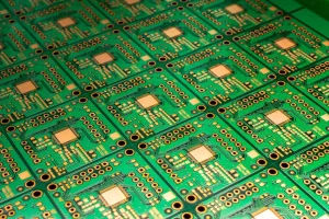
After the nickel layer has been formed, a thin layer of immersion gold is deposited onto the nickel surface through a displacement reaction.
Gold provides excellent resistance to oxidation and corrosion. Because the gold layer protects the nickel surface during storage and assembly, the PCB can maintain a relatively stable surface condition before soldering.
The final ENIG structure therefore combines the barrier and mechanical properties of nickel with the chemical stability of gold.
Key Advantages of ENIG PCB
The combination of nickel and gold provides several characteristics that make Immersion Gold PCB technology suitable for demanding electronic applications.
Excellent Corrosion and Oxidation Resistance
Gold has excellent chemical stability and is highly resistant to oxidation under normal environmental conditions. The nickel barrier layer also helps protect the underlying copper.
This combination can reduce surface oxidation and corrosion during storage, assembly, and operation.
For electronic products exposed to demanding environments, a properly manufactured ENIG finish can contribute to long-term surface stability and reliable electrical connections.
Reliable Electrical Contact
The gold surface provides a stable contact interface for suitable applications such as connectors, contact pads, and other exposed conductive areas.
Although the gold layer itself is relatively thin, its chemical stability helps maintain a clean surface and minimize oxidation-related contact problems.
For high-speed electronic products, however, overall signal performance depends on PCB materials, stack-up, trace geometry, impedance control, and circuit design—not simply the surface finish.
Excellent Surface Flatness
One of the major advantages of ENIG is its relatively flat surface.
Unlike some finishes that can produce more pronounced surface irregularities, ENIG provides a smooth nickel-gold surface that is well suited to fine-pitch components and advanced SMT assembly.
This characteristic is particularly useful for boards using fine-pitch packages, BGA components, and other components where surface uniformity can influence assembly quality.
Good Solderability
A properly controlled ENIG finish can provide a clean and stable surface for soldering.
The gold layer protects the nickel surface before assembly and is consumed or dissolved during soldering under appropriate process conditions, allowing the solder joint to form with the underlying nickel structure.
Consistent surface preparation and plating thickness are essential for maintaining reliable solderability.
Consistent Surface Appearance
Because ENIG is deposited through controlled chemical processes, it can provide a relatively uniform surface across exposed copper areas.
Consistent plating is important for both appearance and manufacturing performance, particularly when a PCB contains numerous fine-pitch pads or complex component patterns.
Applications of Immersion Gold PCB
The characteristics of Immersion Gold PCB make it suitable for applications where surface flatness, corrosion resistance, solderability, and manufacturing consistency are important.
Telecommunications and Networking Equipment
Communication products such as network equipment, routers, switches, optical communication modules, and other high-density electronic systems may use ENIG boards.
These applications often require fine-pitch components, high-density routing, and reliable soldering surfaces.
For more demanding high-speed applications, ENIG can be combined with advanced PCB structures such as multilayer construction, controlled impedance, and high-frequency materials.
Consumer Electronics
Consumer electronics increasingly require compact PCB layouts, fine-pitch components, and reliable SMT assembly.
ENIG is therefore commonly considered for applications such as:
- Smartphones
- Tablets
- Laptops
- Smart devices
- Wearable electronics
- Portable electronic equipment
Its flat surface is particularly beneficial when the PCB uses fine-pitch components or dense component placement.
Industrial Control Systems
Industrial electronics often operate for extended periods and may encounter temperature changes, humidity, vibration, dust, and other environmental conditions.
An appropriate PCB Surface Finish can help protect exposed copper areas while supporting stable assembly and electrical connections.
ENIG may be selected for industrial control boards when a combination of surface protection, solderability, flatness, and long-term storage stability is required.
Medical Electronics
Medical electronic equipment places significant emphasis on manufacturing consistency and reliability.
Circuit boards used in diagnostic equipment, monitoring systems, laboratory instruments, and other medical electronics may require controlled manufacturing processes, appropriate materials, precise fabrication, and reliable surface finishes.
ENIG can be considered when a smooth and stable soldering surface is needed.
Aerospace and Other High-Reliability Electronics
Aerospace, transportation, defense-related electronics, and other demanding applications may require strict control over PCB materials, manufacturing processes, inspection, and traceability.
For these applications, ENIG may be used as part of a broader PCB reliability strategy that includes suitable laminate selection, controlled fabrication, electrical testing, and quality management.
ENIG PCB Manufacturing Quality Requirements
The performance of an ENIG board depends not only on the surface finish itself but also on the quality of the underlying PCB manufacturing process.
Material Selection
The PCB substrate, copper foil, solder mask, plating chemicals, and other production materials should be selected according to the application’s electrical, thermal, mechanical, and environmental requirements.
Different applications may require standard FR-4, high-TG materials, high-frequency laminates, or other specialized PCB materials.
For complex multilayer designs, material compatibility and lamination performance should also be evaluated during engineering review.
Nickel and Gold Thickness Control
Nickel and gold thickness must be controlled according to the PCB design, application, and relevant manufacturing specifications.
Insufficient or inconsistent plating can affect surface protection, solderability, and long-term reliability.
Excessive plating can also increase manufacturing cost without necessarily improving performance.
Therefore, process parameters should be carefully controlled to achieve the required plating characteristics.
Surface Cleanliness
Before chemical deposition, exposed copper surfaces must be properly prepared.
Cleaning and surface activation are important because contamination, oxidation, or inadequate preparation can interfere with the deposition process and lead to uneven plating or adhesion problems.
A controlled pretreatment process helps establish a stable foundation for the nickel and gold layers.
Process Parameter Control
ENIG production requires precise control of chemical parameters such as:
- Bath temperature
- Chemical concentration
- Immersion time
- pH
- Surface preparation
- Deposition rate
- Rinsing conditions
Maintaining stable process conditions helps improve plating uniformity and reduce batch-to-batch variation.
ENIG PCB Inspection and Quality Control
A reliable High Reliability PCB requires quality control throughout the manufacturing process rather than relying solely on final inspection.
Visual Inspection
Visual inspection can identify surface defects such as:
- Uneven plating
- Discoloration
- Scratches
- Contamination
- Surface defects
- Abnormal solder mask conditions
Visual inspection is an important first step in evaluating finished PCB quality.
Plating Thickness Inspection
Nickel and gold thickness can be evaluated using appropriate measurement methods to verify compliance with project specifications.
Consistent plating thickness is important for achieving predictable surface protection and assembly performance.
Electrical Testing
Electrical testing can verify PCB connectivity and identify potential open or short circuits before the boards are delivered for assembly.
For complex circuit boards, electrical testing can be combined with automated optical inspection and other inspection technologies.
Cross-Section Analysis
Cross-section analysis provides a detailed view of the PCB’s internal structure and plated layers.
It can be used to evaluate:
- Copper thickness
- Plated through-hole quality
- Layer alignment
- Dielectric thickness
- Via construction
- Interlayer bonding
- Surface finish structure
This type of analysis can provide valuable information for process verification and reliability evaluation.
ENIG Compared With Other PCB Surface Finishes
Different electronic applications require different surface finishing technologies. ENIG should therefore be evaluated based on the actual requirements of the PCB rather than being considered universally superior.
ENIG vs HASL
HASL uses molten solder to coat exposed copper surfaces and then removes excess solder to create the final finish.
ENIG generally provides a flatter surface than traditional HASL, making it more suitable for fine-pitch components and certain high-density SMT applications.
HASL, however, can remain an economical option for applications with less demanding surface-flatness requirements.
ENIG vs OSP
OSP uses an organic protective coating over exposed copper.
OSP can provide good solderability and may be cost-effective for certain applications, but its protective layer is generally more sensitive to handling and environmental exposure than metallic finishes.
ENIG provides a metallic nickel-gold surface and can offer different durability and storage characteristics.
ENIG vs Immersion Tin
Immersion tin deposits a tin layer over exposed copper and provides a relatively flat surface suitable for SMT assembly.
ENIG offers the additional characteristics of a nickel barrier and gold surface, which may be preferred for applications requiring a more robust metallic surface finish.
The optimal choice depends on PCB design, assembly requirements, expected operating conditions, storage requirements, and project cost targets.
ENIG for Advanced PCB Designs
Modern electronic systems increasingly require higher density, faster signal transmission, and more compact PCB structures.
ENIG can be combined with advanced board technologies to support these requirements.
Multilayer PCB
A Multilayer PCB can integrate multiple conductive layers into a single board, increasing routing capacity and allowing power, ground, and signal layers to be arranged more efficiently.
When ENIG is combined with a properly designed multilayer structure, the finished PCB can support compact and highly integrated electronic systems.
HDI PCB
HDI technology uses microvias, blind vias, buried vias, fine-line routing, and sequential lamination to increase interconnection density.
For compact electronic products, ENIG can be used together with HDI construction to support fine-pitch components and dense SMT layouts.
GOPCBA offers advanced HDI PCB manufacturing solutions for high-density electronic designs, including advanced microvia and interconnection technologies.
High-Speed PCB
For high-speed circuits, surface finish selection should be considered together with the overall PCB structure.
Factors such as dielectric material, trace geometry, layer stack-up, impedance, return paths, and via structures have a much greater influence on high-speed signal integrity than the surface finish alone.
For high-speed designs, engineers can evaluate the complete High-Speed PCB stack-up and impedance-control strategy during the design stage.
How to Choose the Right PCB Surface Finish
Selecting a PCB surface finish requires consideration of several technical and manufacturing factors.
Component and Assembly Requirements
Fine-pitch components, BGA packages, connectors, and other components may have specific surface requirements.
ENIG can be a suitable option when a flat and consistent surface is important for SMT assembly.
Environmental Conditions
Expected temperature, humidity, storage time, corrosion exposure, and operating environment should also be considered.
A suitable surface finish can help protect exposed conductive areas during storage and operation.
Electrical Requirements
For high-frequency and high-speed designs, the complete PCB material system and transmission-line structure should be evaluated.
Surface finish selection should be coordinated with the overall signal-integrity strategy.
Cost Considerations
ENIG generally costs more than some conventional surface finishes because it requires additional chemical processing and metallic layers.
Therefore, engineers should balance performance requirements with production cost and select ENIG when its technical benefits justify the additional manufacturing expense.
Key Manufacturing Takeaways
Keep these items visible during design review and first-article approval.
- How Does ENIG Surface Finish Work: treat this as a repeat-order checkpoint and keep the result with the lot record.
- Key Advantages of ENIG PCB: review the production data and close any deviation before the next build.
- Applications of Immersion Gold PCB: confirm the requirements, process settings and inspection records at first-article approval.
- ENIG PCB Manufacturing Quality Requirements: record the agreed limits and verify them again in the production lot.
- ENIG PCB Inspection and Quality Control: check the drawing, process sheet and inspection plan before release.
- ENIG Compared With Other PCB Surface Finishes: treat this as a repeat-order checkpoint and keep the result with the lot record.
- ENIG for Advanced PCB Designs: review the production data and close any deviation before the next build.
- How to Choose the Right PCB Surface Finish: confirm the requirements, process settings and inspection records at first-article approval.
Conclusion
ENIG PCB technology provides a combination of surface flatness, corrosion resistance, solderability, and surface stability that makes it suitable for many advanced electronic applications.
From telecommunications and consumer electronics to industrial control, medical equipment, and other high-reliability systems, ENIG can provide a reliable surface treatment when properly specified and manufactured.
However, the quality of an ENIG board depends on much more than the gold layer itself. Material selection, copper preparation, nickel and gold deposition, process control, plating thickness, inspection, electrical testing, and overall PCB manufacturing quality all contribute to final performance.
As electronic products continue to move toward miniaturization, higher component density, faster signal transmission, and greater reliability, PCB manufacturers must combine appropriate surface finishing with advanced multilayer, HDI, high-speed, and high-reliability manufacturing technologies.
For customers developing demanding electronic products, GOPCBA provides integrated PCB manufacturing capabilities and engineering support to help select suitable board structures, materials, surface finishes, and production processes according to specific application requirements.