ENIG vs. Hard Gold: 5 Key Differences for PCB Surface Finishes
In PCB Surface Finish selection, ENIG and hard gold are two widely used options. Both finishes can improve oxidation resistance, electrical conductivity, solderability, and contact reliability. However, they differ significantly in their deposition processes, physical characteristics, thickness, durability, cost, and ideal applications.
Choosing the wrong surface finish may lead to unnecessary manufacturing costs, reduced soldering reliability, poor contact performance, or a mismatch between the PCB and its intended application. To make the right decision, engineers and buyers should compare ENIG and hard gold across five important factors: application, surface condition, durability and bonding performance, cost, and compatibility with subsequent assembly processes.
What Is the Difference Between ENIG and Hard Gold?
ENIG, or Electroless Nickel Immersion Gold, is a chemical surface finish that deposits a thin layer of gold over a nickel barrier layer. It is known for its flat and uniform surface, excellent solderability, and strong resistance to oxidation.
Hard gold, typically produced through an electrolytic gold-plating process, uses electrical current to deposit a thicker and more durable gold layer. Because of its superior wear resistance, hard gold is commonly used in areas subject to repeated mechanical contact, such as edge connectors, contact fingers, and certain high-reliability electrical contacts.
Although both processes use gold, they are designed to solve different engineering problems.
1. Application: Choose the Surface Finish Based on Product Requirements
The most important factor in selecting between ENIG and hard gold is the intended application of the PCB.
When ENIG Is the Better Choice
ENIG is widely used for PCBs that require a flat surface, reliable solderability, and good oxidation resistance.
Because the gold layer is thin and uniform, ENIG is particularly suitable for fine-pitch components, BGA packages, high-density circuit boards, communication equipment, precision instruments, medical electronics, and industrial control systems.
For projects requiring stable soldering performance during early-stage product development, Prototype PCB Assembly can benefit from ENIG because its flat surface supports accurate component placement and consistent solder joint formation.
ENIG is also a practical choice when a PCB must maintain solderability during storage before assembly.
When Hard Gold Is the Better Choice
Hard gold is more suitable for applications involving repeated insertion, friction, or mechanical wear.
Typical examples include edge connectors, gold fingers, switches, contact pads, and other areas where the PCB surface will experience frequent physical contact.
Because hard gold can be deposited in a thicker layer and offers better wear resistance, it can provide a longer service life in demanding contact applications.
However, using hard gold on an entire PCB simply because it appears to be a premium finish may significantly increase manufacturing costs without providing additional value.
2. Surface Condition: Flatness Affects Soldering and Contact Reliability
The surface condition of a PCB finish directly affects subsequent assembly and electrical performance.
ENIG Provides a Flat and Uniform Surface
ENIG is known for its smooth and relatively uniform surface.
This characteristic makes it highly suitable for fine-pitch components and high-density layouts. A flat surface can improve solder paste printing and component placement accuracy, helping reduce soldering defects.
For products using
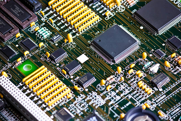
ENIG can provide an excellent foundation for automated surface-mount processes, especially when the design includes small components, fine-pitch packages, or BGA devices.
The uniform surface also helps maintain stable electrical contact performance.
Hard Gold Prioritizes Durability
Hard gold provides a harder and more wear-resistant surface.
Depending on the plating process and PCB geometry, the thickness and surface characteristics may vary across complex areas. However, process optimization can improve plating consistency.
Its primary advantage is not solderability but mechanical durability. Hard gold is therefore generally preferred for designated contact areas rather than solder pads.
When hard gold is applied to areas intended for soldering, excessive gold thickness can create reliability concerns because gold may dissolve into the solder and contribute to brittle intermetallic structures.
3. Durability and Bonding Performance
The durability of a PCB surface finish depends on the deposition process, material structure, thickness, and operating environment.
ENIG for Reliable Environmental Protection
ENIG uses a nickel layer as a barrier between the copper and the immersion gold layer.
The gold protects the nickel from oxidation, while the nickel helps prevent copper migration into the gold layer.
Because ENIG provides good corrosion resistance and a stable surface, it is commonly selected for applications exposed to humidity, temperature changes, and long storage periods.
For many standard PCB Manufacturing projects, ENIG provides a balanced combination of solderability, surface flatness, corrosion resistance, and cost.
Hard Gold for Mechanical Wear Resistance
Hard gold is specifically designed for applications where repeated mechanical contact is expected.
A thicker and harder gold layer can withstand repeated insertion and friction more effectively than ENIG.
This makes hard gold an excellent option for connector contacts and gold fingers.
However, its performance depends heavily on proper process control. Plating current, time, chemistry, and surface preparation must be carefully managed to achieve the required thickness and adhesion.
4. Cost: Comparing Material and Process Requirements
Cost is another major consideration when choosing a PCB surface finish.
ENIG Offers Balanced Performance and Cost
Because the gold layer used in ENIG is relatively thin, gold consumption can be lower than in thick hard-gold applications.
ENIG also offers several performance benefits in a single process, including good solderability, flatness, and oxidation resistance.
For products that require reliable soldering but do not experience repeated mechanical contact, ENIG can provide a cost-effective solution.
Hard Gold Requires More Gold and Process Control
Hard gold generally requires a thicker gold deposit and an electrolytic plating process.
This can increase material consumption, equipment requirements, energy use, and process complexity.
For this reason, hard gold is often applied selectively to specific contact areas rather than across the entire PCB.
In large production programs, unnecessary use of hard gold can significantly increase the overall cost. For High-Volume PCB Assembly, careful surface-finish selection is especially important because even a small increase in cost per board can have a substantial impact on total production expenses.
5. Compatibility with PCB Assembly and Subsequent Processing
The surface finish selected for a PCB must also match the intended assembly process.
ENIG Supports Reliable Soldering
ENIG offers good solderability and can be integrated into a wide range of automated assembly processes.
Its flat surface makes it suitable for solder paste printing and fine-pitch component placement.
When PCBs are stored before assembly, ENIG can also provide good oxidation resistance and help maintain solderability.
This makes it a practical choice for many consumer electronics, industrial systems, communication devices, medical products, and prototype projects.
Hard Gold Should Be Used Carefully Around Soldering Areas
Hard gold is generally more suitable for contact areas than soldering pads.
If a thick gold layer is present in an area that must be soldered, additional process considerations may be required.
The design should therefore clearly define which areas require a durable contact finish and which areas require optimized solderability.
Using the correct finish in the correct location can reduce unnecessary processing and improve overall manufacturing efficiency.
ENIG vs. Hard Gold: A Quick Comparison
Application
ENIG is commonly used for solder pads, fine-pitch components, BGA assemblies, high-density PCBs, and products requiring strong oxidation resistance.
Hard gold is commonly used for edge connectors, gold fingers, switches, and high-wear contact points.
Surface Characteristics
ENIG provides a smooth and flat surface that supports high-precision assembly.
Hard gold provides a harder surface with excellent wear resistance.
Solderability
ENIG is generally well suited for soldering applications.
Hard gold is typically reserved for contact areas and should be carefully controlled when used near soldering locations.
Durability
ENIG offers good environmental stability and corrosion resistance.
Hard gold offers superior mechanical wear resistance.
Cost
ENIG is often more economical for general-purpose soldering applications.
Hard gold can be significantly more expensive when thicker gold layers or large plating areas are required.
How to Choose the Right PCB Surface Finish
ENIG and hard gold are not competing technologies where one is universally better than the other. Each surface finish is designed for different requirements.
Choose ENIG when your project requires:
- Reliable solderability
- A flat surface for fine-pitch components
- Good oxidation resistance
- Compatibility with automated assembly
- Stable performance during storage
Choose hard gold when your project requires:
- Frequent insertion and removal
- High mechanical wear resistance
- Durable connector contacts
- Gold fingers or contact pads
- Long-term performance under repeated friction
The best choice should always be based on the actual operating environment, electrical requirements, mechanical demands, assembly process, and project budget.
Choose the Right Surface Finish for Your PCB Project
Selecting the correct PCB Surface Finish is an important part of PCB design and manufacturing.
A surface finish that is unnecessarily expensive may increase production costs without improving product performance. On the other hand, selecting a finish that cannot withstand the intended operating environment may reduce reliability and shorten product life.
Before making a decision, evaluate whether the PCB requires frequent mechanical contact, high-density assembly, long-term storage, strong oxidation resistance, or specialized electrical performance.
By matching the surface-finish characteristics to the actual application, manufacturers can improve product reliability, optimize production efficiency, and maintain better cost control.
GOPCBA provides integrated PCB manufacturing and assembly solutions for prototypes, low-volume production, and large-scale manufacturing. From PCB fabrication and component sourcing to SMT assembly and final quality control, the right production strategy can help ensure that your selected PCB surface finish performs as intended throughout the product lifecycle.