Fine Line PCB Trace Cost Guide: 3mil, 4mil & 5mil Pricing Analysis
As electronics move toward miniaturization, high speed, and high integration, the demand for fine line PCB trace technology continues to rise. Smartphones, automotive electronics, medical devices, 5G communication equipment, AI hardware, and high-performance computing all require higher density PCB layouts to accommodate more components, faster signal transmission, and more compact form factors.
Traditional PCBs typically use 6mil–10mil trace widths, but advanced electronics increasingly adopt 5mil, 4mil, 3mil, and even ultra‑fine traces. However, finer traces do not mean lower cost. While they reduce copper area, manufacturing complexity increases significantly – including higher LDI (laser direct imaging) precision, tighter etching control, stricter layer registration, lower yields, and elevated inspection standards. Consequently, fine line PCBs are generally more expensive than standard boards.
This guide provides a comprehensive 2026 cost analysis for 3mil, 4mil, and 5mil PCB traces, compares pricing, and explores key factors affecting fine line PCB manufacturing costs, along with practical ways to reduce production expenses.
What Is Fine Line PCB Trace?
PCB traces are copper pathways on the board that connect ICs, resistors, capacitors, power networks, and high‑speed signal channels. Trace width directly impacts current‑carrying capacity, signal integrity, thermal management, routing density, and manufacturing difficulty.
- Standard PCB traces: 6mil–10mil, standard FR‑4, conventional etching – used in industrial controls and general consumer electronics, offering mature processes, low cost, and high yield.
- Fine line PCB traces: 3mil–5mil, requiring high‑precision exposure and tight etching control – used in HDI, smartphone, automotive, and high‑speed communication PCBs, enabling higher density and supporting fine‑pitch components.
- Ultra fine line: Below 3mil, used in semiconductor packaging, AI hardware, and high‑performance computing, requiring HDI technology and advanced manufacturing.
Why Do Finer Traces Cost More?
Many designers assume narrower traces use less copper and should be cheaper. In reality, fine line PCBs cost more due to increased manufacturing precision requirements:
- High‑precision exposure: 3mil and 4mil lines typically require LDI (laser direct imaging) and tight process control. Minimal deviations can cause open circuits, short circuits, impedance anomalies, or signal failure, raising equipment and production costs.
- Tighter etching control: For 3mil/4mil traces, over‑etching can thin lines and increase open‑circuit risk; under‑etching leaves copper residues causing shorts. Stable chemistry and rigorous in‑line inspection are mandatory.
- Lower manufacturing yield: Fine lines demand more inspections, stricter process windows, and higher rework risk, all driving up final unit cost.
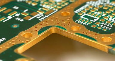
3mil, 4mil, 5mil PCB Trace Cost Comparison (2026)
Prices vary based on board size, layer count, material, quantity, surface finish, and HDI structure. The following are typical market ranges for 2026 (USD).
5mil PCB Trace Cost
5mil is entry‑level fine line technology, suitable for industrial, automotive, communication, and consumer products. Prototype: ~$80–$250 per panel; low‑volume: ~$3–$15 per board; medium‑volume: ~$1–$6 per board. It offers the best cost‑effectiveness for most commercial projects with lower manufacturing risk.
4mil PCB Trace Cost
4mil lines require higher manufacturing capability, used in medical, high‑density industrial, networking, and high‑performance consumer electronics. Prototype: ~$120–$350 per panel; low‑volume: ~$5–$25 per board; medium‑volume: ~$2–$10 per board. Compared to 5mil, 4mil PCBs typically add 15%–35% cost due to tighter registration, stricter testing, and lower yields.
3mil PCB Trace Cost
3mil is advanced fine line technology for HDI, AI devices, smart terminals, high‑speed computing, and avionics. Prototype: ~$200–$600 per panel; low‑volume: ~$10–$50 per board; medium‑volume: ~$5–$20 per board. Relative to standard 6mil lines, 3mil can increase cost by 40%–100% or more, driven by high‑precision equipment, complex processes, and stringent quality control.
Key Factors Affecting Fine Line PCB Cost
- Layer count: Higher layers increase alignment difficulty and manufacturing time. 2‑layer is cheapest; 8‑layer or 12‑layer HDI significantly raises cost.
- Copper weight: Thicker copper (e.g., 2oz vs. 1oz) narrows the etching window, making fine lines harder to control. 3mil with 2oz is much more difficult than 5mil with 1oz.
- Material: Standard FR‑4 is economical; high‑Tg FR‑4, Rogers (RF/5G), and HDI‑specific materials add cost.
- Surface finish: Fine line PCBs often require flatter, more reliable finishes like ENIG (for fine‑pitch components) or ENEPIG (high‑reliability), which cost more than HASL.
Main Applications of Fine Line PCBs
- HDI PCBs: Smartphones, tablets, wearables – require 3–4mil lines and laser microvias.
- Automotive electronics: ADAS, ECU, BMS, smart cockpits – need high reliability and compact size.
- Medical devices: Monitoring, diagnostic, portable equipment – demand stability and miniaturization.
- High‑speed communications: 5G, networking – require low signal loss, impedance control, and high routing density.
How to Reduce Fine Line PCB Manufacturing Costs
- Avoid unnecessarily fine traces: If 5mil meets electrical, signal, and space requirements, choose 5mil to reduce cost, risk, and lead time.
- Optimize stack‑up: Proper signal and power layer planning reduces complexity.
- Partner with a capable manufacturer: An experienced supplier like gopcb can help optimize design, improve yield, and lower overall cost.
gopcb Fine Line PCB Manufacturing Capabilities
As a professional PCB manufacturer, gopcb provides fine line PCB solutions supporting HDI, high‑frequency, automotive, and multilayer boards. With advanced equipment, strict quality systems, and extensive OEM experience, we help global clients achieve high‑density designs, stable mass production, and cost optimization. Whether for prototypes, low‑volume, or high‑volume production, we offer expert engineering support.
Explore our services: PCB manufacturing, prototype PCB assembly, turnkey PCB assembly, low‑volume PCB assembly, and high‑volume PCB assembly.
FAQ: Fine Line PCB Trace Cost
Q1: How much does a 3mil PCB trace cost?
3mil fine line PCBs are typically 40%–100% more expensive than standard boards due to high‑precision exposure, tighter etching, and stricter inspection.
Q2: Is 5mil considered fine line?
Yes, 5mil is generally regarded as fine line technology and is the most cost‑effective choice for many commercial applications.
Q3: What is the minimum PCB trace width achievable?
Advanced manufacturers can achieve 3mil or even smaller. HDI and advanced packaging can go to sub‑2mil levels.
Q4: Does finer trace reduce current capacity?
Yes. Finer traces have lower current‑carrying capability and higher resistance, increasing heat generation. Design must account for copper weight, trace length, operating current, and thermal management.
Q5: Which trace width offers the lowest cost?
Generally, 5mil provides the best cost‑performance balance; 4mil suits high‑density designs; 3mil is reserved for high‑end HDI applications.
Conclusion: How to Choose the Right Fine Line PCB Trace
Fine line PCB technology drives electronics toward smaller size, higher performance, and greater functionality. In 2026, 5mil remains the most cost‑effective option for most commercial projects; 4mil fits high‑density electronics; 3mil is ideal for HDI, high‑speed, and high‑performance applications. When selecting trace width, do not pursue the minimum size alone – consider product requirements, manufacturing capability, cost budget, and long‑term reliability. As a professional PCB manufacturer, gopcb offers full fine line PCB services from prototyping to mass production, delivering high‑reliability, cost‑effective solutions for global customers.