Four-Layer PCB Stack Arrangements and Trade-Offs
A four-layer board is the point at which a printed circuit stops being a wiring carrier and starts being a controlled electrical environment. Adding two inner layers gives the designer a ground plane and a power plane, and those two elements change the behaviour of every trace on the board. Most digital designs that are currently built on two layers would be simpler, quieter and often cheaper to produce on four.
This article explains what the extra layers actually provide, how the layers should be arranged, and the situations where four layers are still not enough.
What the Inner Layers Provide
The first benefit is a reference plane. Every signal trace on a four-layer PCB with ground on layer two has a return path directly beneath it, so the loop area between the outgoing and returning currents is small. That reduces radiation, reduces susceptibility and gives the trace a defined characteristic impedance instead of one that changes with whatever happens to be routed nearby.
The second benefit is power distribution. A power plane distributes the supply with a very low inductance compared with a trace network, and the capacitance between the power plane and the adjacent ground plane supplies high-frequency energy close to the devices that need it. Both effects are difficult to obtain any other way.

The Three Common Arrangements
The conventional stack arrangement is signal, ground, power, signal. It is cheap to build and it gives both outer layers a reference plane, which is why it dominates four-layer designs. Its weakness is the spacing between the power and ground planes, which on a 1.6 mm board is large enough to make the distributed capacitance modest.
The second arrangement places ground on both outer layers and runs signals and power on the inner layers, using wide traces for the power. This gives the best shielding and the smallest loop area, because every outer-layer signal is referenced to an outer-layer ground. It only works where the component density is low enough to leave copper area free, since the signals now share the inner layers with the power distribution.
Return Paths and Plane Splits
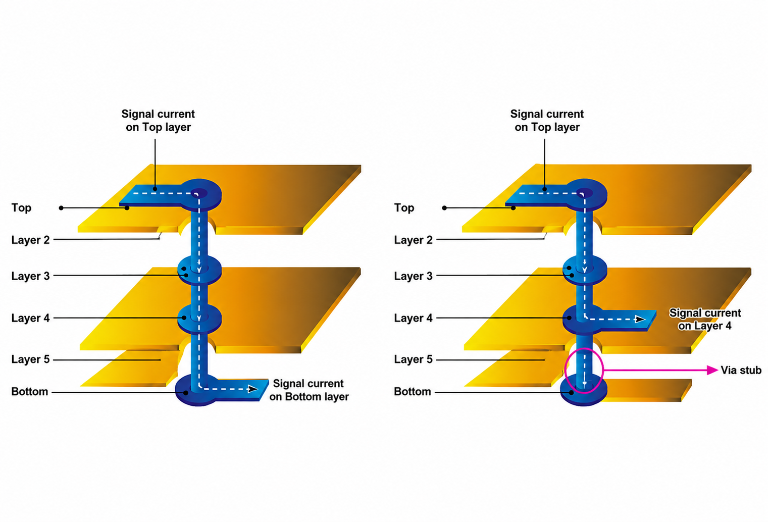
The value of the plane depends entirely on its continuity. A ground plane that is cut by a slot or by a row of vias forces the return current to divert around the obstruction, and the loop area increases by the length of the detour. At the frequencies where four-layer boards are typically used, that diversion is the difference between a quiet design and one that fails emissions testing.
Where a split is unavoidable, the high-speed traces should be routed so that they do not cross it, or a stitching capacitor should be placed at the crossing to give the return current a path. The layer stack reference for one to eight layers describes how the arrangement changes as the count rises, and the prototype build requirements cover the documentation the fabricator needs to produce a controlled-impedance four-layer board.
Impedance Control on Four Layers
A four-layer board can be built with controlled impedance, and it usually should be. The dielectric thickness between the outer layer and the ground plane determines the trace width for a given impedance, and on a standard 1.6 mm board with 0.2 mm of dielectric that width is around 0.35 mm for 50 ohms.
The tolerance is the part that has to be specified. The dielectric thickness varies with the laminate and the process, and a variation of ten percent produces a similar order of variation in impedance. Specifying the target impedance and letting the fabricator adjust the artwork is more reliable than specifying a trace width and hoping the stack matches.
Cost Compared With Two Layers
A four-layer board costs more than a two-layer board of the same size, and the difference is smaller than most people expect. The material cost roughly doubles, but the processing cost is dominated by setup, drilling and testing rather than by the number of layers for a simple design.
The savings on the other side are often larger. A four-layer board frequently needs fewer components, because the decoupling and filtering that a two-layer design requires are partly provided by the planes. It also takes less engineering time to route, because the return paths do not have to be planned trace by trace. On a design of any complexity the total cost usually favours four layers.
Where Four Layers Are Not Enough
Four layers run out of capacity when the routing demand exceeds what two signal layers can carry. A fine-pitch ball grid array with several hundred connections cannot be escaped on two signal layers, and a board with several high-speed buses plus a wide memory interface usually needs six or more.
The sign that four layers are no longer sufficient usually appears as unroutable connections after the placement is final, or as a design that routes only by violating the rules. Adding two layers at that point is cheaper than accepting a layout with compromised return paths, and it is worth planning the stack with the possibility of a six-layer version in mind.
Decisions to Make Early
The layer assignment, the dielectric thicknesses and the impedance targets should be fixed before routing begins, because changing them later invalidates every controlled-impedance trace. The component placement should also be reviewed against the plane arrangement, since a device placed over a split in the plane loses the benefit of the plane entirely.
Two further decisions belong in the same review. The first is whether the design needs a controlled-impedance coupon on the panel, which is worth ordering on any board where the impedance matters. The second is the surface finish, which affects the fine-pitch assembly and should be chosen with the pad geometry rather than after the layout is complete.
A third decision concerns the ground strategy at the connectors. Every cable that enters the board carries a return, and that return has to reach the ground plane through a low-inductance path rather than through a narrow trace. Providing a wide contact area or several vias at each connector, and keeping that path clear of the sensitive sections, is easier to arrange before the layout than to add afterwards. The general manufacturable design rules cover the dimensional side of the same set of choices.
FAQ
Is a four-layer board worth it for a simple design? Where the design has any fast edges or any analogue section, yes. The plane provides a defined return path that a two-layer board cannot, and the improvement in emissions is often enough to justify the cost on its own.
Can four layers support differential pairs? Yes, provided the pairs are routed on the outer layers with a continuous reference beneath them and the spacing is held. The main constraint is routing capacity rather than electrical performance.
What is the maximum board thickness for four layers? There is no hard limit, but a thicker board means a larger distance between the outer layers and the inner planes, which increases the trace width needed for an impedance target. Very thick four-layer boards are usually better built as six layers with thinner dielectrics, because the impedance calculation becomes difficult to satisfy and the trace widths grow beyond what the layout can accommodate.