HDI Multilayer Circuit Board: Technology, Manufacturing and Applications
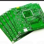
An HDI multilayer circuit board is a high density interconnect PCB built with microvias, fine lines, and multiple build-up layers. It allows designers to place many components and signals in a smaller area than a conventional multilayer board. As electronic products become thinner, faster, and more powerful, the HDI multilayer circuit board has become a core technology in smartphones, automotive electronics, 5G equipment, medical instruments, and other advanced systems.
HDI boards achieve their performance through special manufacturing methods. Blind vias connect an outer layer to an inner layer without passing through the whole board. Buried vias connect only internal layers. Microvias created by laser drilling can be very small, while build-up lamination adds routing layers one at a time. These features give the designer more flexibility and improve the electrical behavior of the final board.
High Wiring Density in a Smaller Board
The most obvious advantage of an HDI multilayer circuit board is density. Modern HDI designs may use holes with a diameter of 0.1 mm or smaller and line widths and spacing close to 30 micrometers. The fine structures allow many traces to pass through a compact area, which is essential when hundreds of components must fit on one board.
In a smartphone main board, the HDI multilayer circuit board connects processors, memory, RF chips, cameras, and power management circuits in a very small space. The board area can be reduced while maintaining the routing needed for complex functions. This makes devices thinner and lighter and gives industrial designers more room for batteries, cameras, and antennas.
Density is also valuable in non-consumer products. Medical devices, communication modules, automotive controllers, and industrial sensors often need more functionality in a limited enclosure. High layer count combined with microvias can reduce the number of separate boards and connectors required by the product.
Signal Integrity for High-Speed Electronics
Electronic systems are moving data faster than ever. 5G, Wi-Fi, USB, PCIe, and high-speed memory interfaces require clean signals from one component to another. An HDI multilayer circuit board helps preserve signal quality by keeping traces short and by using controlled impedance.
Blind vias and buried vias reduce the parasitic effects caused by long through-hole stubs. A shorter vertical connection creates less inductance and capacitance, which means less signal distortion at high frequency. Low-loss materials may be used in the stackup to reduce attenuation in critical high-speed paths.
HDI boards also support controlled impedance designs. Trace width, spacing, dielectric thickness, and reference plane placement can be tuned for a specific impedance target. This is important for millimeter-wave signals in 5G, differential pairs in high-speed interfaces, and RF circuits that need predictable transmission behavior.
Flexible Interconnection Structures
An HDI multilayer circuit board can combine several via types in one design. Blind vias start on an outer layer and stop at an inner layer. Buried vias connect only internal layers and are added during the build-up process. Through vias pass completely through the board and may be used for power or other connections.
This combination improves routing efficiency. A signal that needs to travel from the top layer to the second layer can use a short blind via instead of a long through hole. An internal connection between two signal layers can use a buried via, leaving more room on the outer layers for components.
Stacked vias can increase density further by placing microvias directly above one another. Staggered vias are offset for simpler manufacturing. The choice depends on the required routing density, reliability target, and cost of the board.
Build-Up Technology
The core of HDI multilayer circuit board production is build-up lamination. Instead of pressing all layers in one large stack, the manufacturer starts with a core and adds dielectric material and copper layers one step at a time. Each build-up step creates a new layer with microvias and fine circuitry.
During each cycle, laser drilling creates small holes in the dielectric. The holes are cleaned and plated with copper to connect the new layer to the layer below. Photolithography and etching then form the circuit pattern on the new surface. Repeating this process adds more routing layers and increases density.
Build-up lamination gives the manufacturer precise control over layer thickness and alignment. It also allows the use of different materials at different stages, which can improve electrical or thermal performance. The process is more complex than conventional multilayer production, but it creates the structure that HDI designs require.
Laser Drilling for Microvias
Laser drilling is one of the most important processes in HDI manufacturing. A laser beam can create very small, accurately positioned holes in dielectric material. This is necessary because mechanical drills are too large for microvias and may damage delicate laminates.
Laser drilling produces smooth hole walls and can be used for different material types. The process parameters must be matched to the thickness and composition of the dielectric. If the laser is too strong or too weak, the via shape may be poor, which can affect plating and reliability.
After drilling, the holes must be cleaned to remove residue. A clean, well-shaped microvia is easier to plate with copper and creates a stronger electrical connection. In high-layer HDI boards, every microvia should be inspected to avoid defects that are difficult to find after lamination.
Plating and Surface Finish
Copper plating is critical in HDI multilayer circuit boards. Blind and buried vias must be filled or plated with enough copper to carry current and survive thermal cycling. Via filling improves the reliability of stacked structures and provides a flat surface for component mounting or additional build-up layers.
Plating thickness must be controlled through the entire board, especially in deep holes and small microvias. Uneven plating can increase resistance or cause voids. A consistent plating process reduces the risk of connection failure during the life of the product.
Surface finish protects the exposed copper and provides a solderable surface. Common finishes include ENIG, immersion silver, and organic solderability preservative. The finish should be selected based on assembly method, storage time, and environmental requirements.
Applications in Smartphones and Consumer Electronics
Smartphones are among the largest users of HDI multilayer circuit boards. A modern phone contains a powerful processor, high-speed memory, cellular and Wi-Fi radios, camera modules, display drivers, audio circuits, and power management. All of these functions must fit into a thin, compact chassis.
The HDI main board provides the routing density needed for this integration. It also supports high-speed signals used by 5G modems and other advanced interfaces. Because the board can be smaller, the phone can devote more space to the battery, display, or camera system.
Wearable devices, tablets, and compact consumer modules use the same technology to reduce size and weight. HDI helps product teams create devices that are easier to carry and more comfortable to wear.
Automotive HDI Multilayer Applications
Automotive electronics are becoming more complex as vehicles add ADAS, connectivity, and electric powertrain functions. Engine control, infotainment, sensor modules, and autonomous driving computers need reliable boards that can operate in high temperature and high vibration environments.
An HDI multilayer circuit board helps automotive designers pack more processing power into compact controller enclosures. The short interconnect paths improve signal timing and reduce noise, which is important for camera and radar data used by safety systems.
Automotive HDI boards may use materials with higher thermal endurance and stronger mechanical properties. The manufacturing process must control material shrinkage and layer registration so that the board remains reliable over many years of service.
5G Communication Equipment
5G networks use higher frequencies and more complex antenna systems than previous generations. Base stations, routers, and switches need boards that can carry large amounts of high-speed data while keeping signal loss low.
HDI multilayer circuit boards are used in RF modules, digital processing boards, and network equipment because they provide precise routing and good high-frequency behavior. The boards support small vias and fine traces that are difficult to achieve with conventional manufacturing.
Low-loss materials may be combined with HDI structures for millimeter-wave circuits. Careful impedance control and short transitions help the system maintain the signal quality required for high-speed 5G communication.
Medical Electronics and High-Reliability Systems
Medical imaging equipment, patient monitors, and diagnostic instruments demand high precision and long-term reliability. HDI multilayer circuit boards help these systems achieve the required density and electrical performance in a compact design.
MRI, CT, and ultrasound systems process very large amounts of data while detecting small signals. A clean power and ground design on an HDI board reduces noise that could affect image quality. The board also helps manufacturers reduce the size of portable devices.
Because medical products must be safe, the board materials and processes should be qualified for the intended application. Traceability of materials and production records supports quality audits and long-term field support.
Working with an HDI Manufacturer
HDI multilayer circuit board projects should begin with a clear stackup. The number of build-up cycles, microvia structure, material selection, and impedance requirements should be decided before layout begins. A design review with the manufacturer can identify practical limitations and cost drivers.
PCB design and layout services can help optimize the HDI stackup and routing for manufacturing. Once the design is ready, PCB manufacturing must control laser drilling, plating, lamination, and testing across every layer.
During prototyping, prototype PCB assembly validates the board with real components. For volume production, turnkey PCB assembly and component procurement create a smoother path from design to finished product.
Conclusion
The HDI multilayer circuit board is a key technology for modern electronic products that need high density, high speed, and compact size. It combines microvia interconnection, fine-line routing, and multiple build-up layers to support advanced processors, communication modules, and sensing systems.
Successful HDI production depends on precise design and disciplined manufacturing. By choosing the right stackup, materials, and manufacturing partner, engineers can create boards that deliver strong performance and long-term reliability for the demanding electronic systems of today and tomorrow.