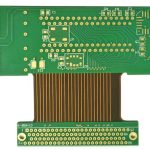
High Density Printed Circuit Board: HDI Technology and Manufacturing
A high density printed circuit board connects more components, signals, and power paths in a smaller space than a conventional board. It acts like a precision traffic hub inside an electronic product, directing data between processors, memory, sensors, radios, and other circuits. As electronic devices become smaller and more powerful, high density PCB technology has become essential in communication, medical, aerospace, and computing systems.
High density printed circuit boards are usually built with HDI technology. This means the board uses fine lines, small microvias, blind vias, buried vias, and multiple build-up layers to achieve more routing in less area. Understanding how these boards are designed and manufactured helps engineers choose the right technology and supplier.
The Evolution of High Density PCB Technology
High density interconnect technology began to develop in the 1960s, when engineers first looked for ways to increase circuit density. Over the following decades, digital electronics, communications, and automation demanded smaller boards with more functions. Manufacturers responded by reducing hole size, trace width, and component spacing.
Modern HDI technology has moved beyond simple microvia boards. Advanced products use ultra-thin layers, internal vias, stacked microvias, and fine-line processes to increase the three-dimensional density of the circuit. These structures allow high-performance devices to fit into products that would have been impossible with older PCB technology.
The evolution continues as 5G, artificial intelligence, and high-speed computing create new requirements for bandwidth, signal quality, and thermal management.
Higher Routing Density and Finer Lines
The main benefit of a high density printed circuit board is routing density. More traces can fit in the same area, which allows the designer to connect more components without making the board larger. This is particularly useful for processors, memory, and RF modules that need many parallel signals.
Advanced HDI boards can produce line widths and spacing of 25 micrometers or less. Fine lines require high-resolution imaging, controlled etching, and clean production conditions. When line width is reduced, even small defects can cause opens or shorts, so the manufacturing process must be stable.
High density also helps reduce the size and weight of the final product. A smaller board may fit in a thinner smartphone, a more compact wearable, or a lighter satellite module. This creates new design opportunities for product teams.
Microvias and Interconnection
Microvias are one of the defining features of a high density printed circuit board. A microvia is usually smaller than 150 micrometers in diameter. It connects one layer to another through a small, laser-drilled hole. Because microvias are short, they reduce signal delay and parasitic effects compared with long through-hole connections.
Microvias also increase assembly density. They allow components to be placed over routing areas and reduce the number of large holes that consume space. The result is a more compact board with more available routing area.
Different via structures are used for different functions. A blind via connects an outer layer to one or more internal layers. A buried via is hidden entirely inside the board. Through vias pass completely through the stackup. The combination of these structures gives the designer more freedom to optimize the layout.
Signal Integrity at High Speed
High-speed signals need predictable impedance and low loss. A high density printed circuit board can use stripline or microstrip structures to control the signal path. The designer chooses the trace layer, distance to ground, and dielectric material to achieve the target impedance.
Low-dielectric-constant and low-loss materials reduce signal attenuation and delay. This is especially important for millimeter-wave 5G, high-speed memory, and serial data links. The board should also minimize unwanted radiation so that the product passes electromagnetic compatibility testing.
Short interconnects created by microvias reduce the chance of reflections and timing errors. When high-speed signals travel through fewer and shorter transitions, the system is easier to design and more reliable in production.
Materials Used in High Density PCBs
High density boards use materials with good electrical and thermal properties. FR-4 is common for many consumer and industrial designs, while low-loss laminates are used for high-frequency circuits. Polyimide may be selected for high-temperature or flexible applications.
Material dimensional stability is important during lamination. If the laminate expands or shrinks unevenly, layer registration can be lost. Dielectric constant consistency also affects impedance control. The manufacturer must choose materials that process well together.
Copper foil quality affects fine-line etching and high-frequency loss. The copper surface should be smooth enough for good signal performance but provide enough adhesion for reliable lamination. Bonding film and prepreg must also meet the requirements of the build-up process.
Inner Layer Processing
The inner layers of a high density printed circuit board form the foundation of the finished structure. The circuit pattern is transferred to the copper surface using laser direct imaging or photolithography. This creates the precise image needed for fine-line etching.
Chemical etching removes the unwanted copper and leaves the circuit traces. Etching time, temperature, and chemistry must be controlled to prevent undercut. After etching, the layer is cleaned and inspected before lamination.
Multiple process steps may be needed to build thin layers with small features. Each layer must be measured and checked so that the final board meets its electrical and mechanical requirements.
Lamination and Layer Alignment
High density boards are formed by aligning inner layers with insulating prepreg and pressing them under high temperature and pressure. The alignment must be accurate across the whole panel. Any layer shift can cause a via to miss its target pad.
The lamination profile must match the materials. Temperature, pressure, vacuum, and time control the flow of resin and the final board thickness. Slow cooling can reduce internal stress and prevent warpage in a thin, high-layer board.
After lamination, additional build-up cycles may be used to add more routing layers. Each cycle increases complexity, so the manufacturer must maintain precise registration through every step.
Drilling and Copper Plating
Microvia holes are usually created by laser drilling because they are too small for mechanical drills. The laser parameters are adjusted for the material and hole depth. Clean, well-shaped holes are needed for reliable plating.
After drilling, the board goes through electroless and electrolytic copper plating. The copper must fill or coat the microvias with enough thickness to carry current. Plating quality is especially important in stacked via structures.
For high-density boards, surface finishes such as ENIG, immersion silver, OSP, or hard gold may be applied. The finish protects the copper and provides a solderable surface for component assembly. The choice depends on the application and assembly process.
Testing and Inspection
High density printed circuit boards require thorough testing because defects are difficult to find after assembly. Automated optical inspection checks trace patterns and surface defects. X-ray inspection can verify internal alignment and hidden via structures.
Electrical testing checks for opens, shorts, and correct circuit continuity. Flying probe testing is useful for prototypes and small batches, while fixture testing can be faster for high-volume boards. Impedance testing confirms that critical signal traces meet the design target.
Some advanced boards need microsection analysis to inspect plating thickness, via filling, and layer-to-layer connections. Environmental testing can simulate the temperature and humidity conditions of the final product.
Applications in 5G and Mobile Devices
5G base stations process large amounts of data and need boards with low loss and high signal quality. A high density printed circuit board supports the RF modules, baseband processing, and high-speed interfaces used in the network. It also helps reduce the size of radio equipment.
Smartphones and other mobile devices use HDI boards to integrate processors, memory, 5G modems, cameras, and power circuits in a very small area. The high routing density allows the product to remain thin while providing advanced functions.
As mobile products add more antennas and sensors, the board must manage additional signal paths and electromagnetic interference. High density PCB technology gives designers the flexibility needed to meet these challenges.
Medical, Aerospace, and AI Applications
Medical imaging equipment, monitors, and diagnostic devices need precise, reliable electronics. A high density printed circuit board allows the device to be smaller and lighter while maintaining signal quality. Portable and home-care products also benefit from reduced board size.
Aerospace systems face strict limits on weight and volume. Satellites, aircraft electronics, and navigation systems use HDI boards to fit complex functions into compact modules. The boards must remain reliable in extreme environments and over long service lives.
Artificial intelligence servers use multiple processors and accelerators that communicate at very high speed. High density printed circuit boards support the dense routing and clean signal paths required for AI training and inference. They help connect GPUs, memory, and network devices with low latency.
Working with a High Density PCB Supplier
A high density printed circuit board project should begin with a clear stackup and design review. The number of layers, via structure, material system, and impedance targets must be defined early. The manufacturer can then recommend process limits and cost-effective options.
PCB design and layout review helps optimize the HDI structure for manufacturability. Once the design is complete, PCB manufacturing must control imaging, etching, lamination, drilling, plating, and testing across every layer.
During product development, prototype PCB assembly can validate the board with real components. When production volume increases, turnkey PCB assembly and component procurement provide an integrated path from bare board to finished electronic module.
Conclusion
The high density printed circuit board is a foundation technology for compact, high-performance electronics. It combines fine traces, microvias, build-up layers, and controlled impedance to support advanced communication, computing, medical, and aerospace systems.
Successful HDI production depends on careful design, precise materials, and disciplined manufacturing. By working with an experienced high density PCB supplier, engineers can create boards that deliver the density and reliability required by tomorrow’s products.