As electronic systems continue to operate at higher frequencies and data rates, conventional PCB materials are increasingly challenged by signal loss, impedance variation, thermal stress, and manufacturing requirements.
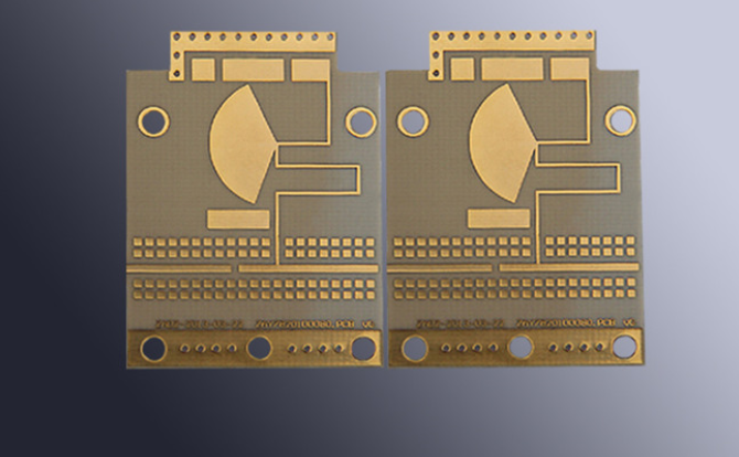
High-Frequency PCB Materials are specially engineered substrates designed to provide stable electrical performance at RF, microwave, and other high-frequency operating ranges.
In general, high-frequency applications are commonly associated with frequencies above several hundred megahertz, while RF and microwave designs may extend into the GHz range and beyond. However, there is no single frequency boundary that universally defines a high-frequency PCB. The appropriate material depends on signal rise time, operating frequency, bandwidth, transmission-line length, power level, and application requirements.
Modern applications such as wireless communication, radar, satellite systems, automotive radar, 5G infrastructure, and high-speed networking increasingly require advanced PCB Materials with controlled dielectric properties and low signal loss.
Why High-Frequency PCB Materials Are Important
At low frequencies, conventional FR-4 materials are suitable for many electronic products. As frequency increases, however, dielectric loss and conductor loss become increasingly important.
A PCB transmission line is not simply a copper trace. Its electrical behavior depends on the relationship between the conductor, dielectric material, reference plane, geometry, and surrounding environment.
Important material parameters include:
- Dielectric constant (Dk)
- Dissipation factor (Df)
- Dielectric thickness
- Thermal expansion
- Moisture absorption
- Dimensional stability
- Copper surface roughness
- Thermal performance
For high-speed and RF designs, changes in these properties can affect impedance, propagation delay, insertion loss, phase behavior, and signal integrity.
Therefore, choosing suitable High-Frequency PCB Materials should be part of the initial PCB design process rather than an afterthought.
Main Types of High-Frequency PCB Materials
High-frequency laminates can be broadly classified according to their resin systems and reinforcement structures.
Common categories include:
- Ceramic-filled thermoset materials
- PTFE-based materials
- Hydrocarbon/ceramic laminates
- Low-loss modified epoxy systems
- Other specialized RF and microwave laminates
Each material category has different electrical, thermal, mechanical, and manufacturing characteristics.
1. Ceramic-Filled Thermoset Materials
Ceramic-filled thermoset laminates combine a thermosetting resin system with ceramic fillers and reinforcement materials.
These materials are designed to provide more stable dielectric properties than many conventional PCB laminates while maintaining relatively practical manufacturing characteristics.
Typical advantages include:
- Stable dielectric constant
- Low dielectric loss
- Good dimensional stability
- Good thermal performance
- Suitable mechanical strength
- Compatibility with multilayer PCB manufacturing
Ceramic-filled materials can be useful for RF filters, antennas, power amplifiers, and other microwave circuits.
However, the presence of ceramic fillers may influence mechanical processing. Compared with standard FR-4, some ceramic-filled laminates can be more abrasive or brittle, requiring optimized drilling and routing parameters.
2. PTFE PCB Materials
PTFE, or polytetrafluoroethylene, is widely used in demanding RF and microwave applications because of its low dielectric loss and favorable high-frequency electrical properties.
PTFE PCB materials can provide excellent performance at microwave frequencies, but they generally require more specialized processing than conventional epoxy/glass laminates.
Important characteristics include:
- Very low dielectric loss
- Stable RF performance
- Low moisture absorption
- Suitable dielectric properties for microwave circuits
However, PTFE is mechanically softer than many conventional thermoset PCB materials. This can create additional challenges during cutting, drilling, plating, and lamination.
Therefore, manufacturers need to establish appropriate process parameters before mass production.
PTFE PCB Processing Considerations
Material Cutting
During cutting, the PCB surface should be protected from scratches, dents, and mechanical deformation.
Protective films or suitable handling methods can be used when necessary.
Because PTFE-based materials can behave differently from standard FR-4 during machining, excessive mechanical stress should be avoided.
Drilling
Drilling is one of the most important processing steps for PTFE-based High-Frequency PCB materials.
Appropriate drill selection and process parameters should be established according to:
- Finished hole diameter
- Board thickness
- Material construction
- Copper thickness
- Drill geometry
- Spindle speed
- Feed rate
- Stack height
Using worn drill bits can increase burr formation and negatively affect hole-wall quality.
Therefore, drill quality should be monitored based on actual hole-wall condition rather than tool-hit count alone.
Hole-Wall Treatment
PTFE has low surface energy and is chemically different from conventional epoxy/glass materials.
As a result, achieving reliable copper adhesion inside drilled holes may require specialized surface activation or treatment.
Depending on the material construction and manufacturer’s process, plasma treatment or other surface-activation technologies may be used before electroless copper deposition.
Proper hole preparation is essential for reliable plated through-hole performance.
PTH and Copper Plating
After drilling and hole preparation, plated through-hole processing creates electrical connections between PCB layers.
The general sequence may include:
- Hole cleaning
- Surface conditioning
- Activation
- Electroless copper deposition
- Electrolytic copper plating
- Thickness inspection
The exact chemistry and process conditions depend on the laminate system and the PCB manufacturer’s process capability.
For PCB Manufacturing, consistent hole-wall preparation and copper adhesion are particularly important for RF multilayer boards because poor plating reliability can affect both electrical continuity and long-term mechanical reliability.
Solder Mask Processing
Applying solder mask to high-frequency materials requires appropriate surface preparation.
The process may include:
- Surface cleaning
- Chemical pretreatment
- Solder mask coating
- Exposure
- Development
- Thermal curing
- Final inspection
Mechanical abrasion should be selected carefully because some high-frequency laminates can have different surface characteristics from standard FR-4.
The solder mask material and thickness can also influence RF performance in certain controlled-impedance structures. For demanding RF designs, designers should consider whether the solder mask covers the transmission line and whether its dielectric properties need to be included in simulation.
Routing and Mechanical Processing
Routing high-frequency PCB materials requires appropriate tooling and support.
During routing:
- The board should be securely supported.
- Excessive mechanical stress should be avoided.
- Tool wear should be monitored.
- Burr formation should be controlled.
- Finished dimensions should be inspected.
For PTFE and ceramic-filled materials, routing parameters may need to differ from standard FR-4.
Manufacturers should therefore establish process windows through trial production before releasing the product to volume manufacturing.
Dk: Dielectric Constant
Dk, or dielectric constant, is one of the most important parameters when selecting PCB Materials for high-frequency applications.
Dk affects:
- Signal propagation velocity
- Transmission-line impedance
- Electrical wavelength
- Phase delay
- Antenna dimensions
- Filter characteristics
However, the Dk value listed on a material datasheet should not automatically be treated as a universal constant.
Dk can vary depending on:
- Measurement method
- Frequency
- Resin content
- Glass weave
- Material construction
- Temperature
- Moisture
- Orientation
Therefore, designers should use appropriate material data for the actual frequency range and PCB construction.
Df: Dissipation Factor
Df, or dissipation factor, represents dielectric loss.
As signal frequency increases, dielectric loss can become an important component of total transmission loss.
A lower Df generally means lower dielectric loss, making low-Df materials attractive for long transmission lines, RF circuits, microwave filters, and high-speed digital channels.
However, Df should not be evaluated independently.
Total PCB signal loss also depends on:
- Copper roughness
- Copper thickness
- Trace geometry
- Frequency
- Dielectric thickness
- Transmission-line length
- Via transitions
- Connector transitions
For this reason, engineers should evaluate the complete channel rather than selecting a material based solely on its Df value.

Frequency Stability of Dk and Df
One of the most important differences between conventional and advanced High-Frequency PCB Materials is the stability of their electrical properties across frequency.
Some conventional PCB materials exhibit noticeable changes in Dk and Df as frequency increases.
This can make impedance calculations and high-frequency simulations less predictable.
Advanced RF laminates are generally designed to provide more stable dielectric characteristics over their specified operating frequency range.
This is particularly important for:
- Broadband RF circuits
- High-speed digital channels
- Antennas
- Filters
- Radar systems
- Communication equipment
Designers should therefore review the frequency-dependent Dk and Df data provided by the material manufacturer instead of relying on a single nominal value.
Why Df Is Particularly Important
For many high-frequency applications, Df deserves particular attention because dielectric loss generally becomes more significant as frequency increases.
A material with a relatively stable Dk but a high Df may still produce excessive insertion loss.
Therefore, when comparing materials, engineers should consider:
- Nominal Df
- Frequency-dependent Df
- Df tolerance
- Temperature dependence
- Moisture dependence
- Manufacturing variation
The lower the allowable signal-loss budget, the more important these factors become.
High-Frequency PCB Material Selection
Selecting the correct High-Frequency PCB Materials requires a balance between electrical performance, manufacturing capability, reliability, and cost.
The following factors should be evaluated:
Electrical Requirements
Determine:
- Operating frequency
- Signal bandwidth
- Required impedance
- Allowable insertion loss
- Dk requirements
- Df requirements
Mechanical Requirements
Consider:
- Board thickness
- Layer count
- Drill requirements
- Routing requirements
- Dimensional stability
- Mechanical strength
Thermal Requirements
Evaluate:
- Operating temperature
- Tg
- Td
- CTE
- Thermal cycling
- Power density
Manufacturing Requirements
Confirm whether the manufacturer can reliably process the selected material using the required:
- Drilling
- Lamination
- Plating
- Imaging
- Etching
- Solder mask
- Surface finish
- Electrical testing
Cost Requirements
Advanced high-frequency materials can be considerably more expensive than standard FR-4.
Therefore, designers should avoid using specialized materials unless their electrical or reliability advantages are actually required by the application.
High-Frequency PCB vs. Conventional FR-4
FR-4 remains an excellent general-purpose PCB material and is suitable for many digital and electronic applications.
However, specialized High-Frequency PCB materials may be required when the design has demanding RF or high-speed requirements.
| Characteristic | Conventional FR-4 | High-Frequency Materials |
|---|---|---|
| General-purpose applications | Excellent | Application dependent |
| High-frequency loss | Moderate to high depending on grade | Generally lower |
| Dk stability | Material dependent | Typically optimized |
| Df | Higher for many grades | Generally lower |
| RF applications | Limited for demanding designs | Well suited |
| Manufacturing | Very mature | Material dependent |
| Cost | Lower | Generally higher |
The correct choice depends on the actual electrical requirements rather than simply the operating frequency.
Simulation and Material Selection
For high-speed and RF applications, simulation should be performed before finalizing the PCB stack-up.
Engineers can use electromagnetic and signal-integrity simulations to evaluate:
- Characteristic impedance
- Insertion loss
- Return loss
- Crosstalk
- Propagation delay
- Phase response
- Current distribution
The simulation model should use realistic material parameters whenever possible.
For example, using an inaccurate Dk value can lead to an incorrect trace width or dielectric thickness during impedance design.
Therefore, accurate material data is an important part of successful PCB Manufacturing.
Kingda’s High-Frequency PCB Manufacturing Considerations
For demanding RF PCB projects, material selection and manufacturing capability should be evaluated together.
Kingda can support high-frequency PCB projects by coordinating material selection with stack-up design and manufacturing process control.
Key considerations include:
- High-frequency laminate processing
- PTFE PCB manufacturing
- Ceramic-filled laminate fabrication
- Controlled impedance production
- Precision drilling
- Multilayer lamination
- Copper plating
- Fine-line fabrication
- Surface finishing
- Electrical testing
- RF performance considerations
Early communication between the PCB designer and manufacturer helps determine whether the selected material and stack-up can be manufactured consistently.
This is particularly important for PTFE and ceramic-filled laminates because their mechanical and thermal behavior may differ from conventional FR-4.
Conclusion
High-Frequency PCB Materials are essential for RF, microwave, high-speed communication, radar, antenna, and other demanding electronic applications.
PTFE-based materials provide excellent low-loss RF performance but may require specialized manufacturing processes. Ceramic-filled thermoset materials offer a useful balance between high-frequency electrical characteristics and relatively conventional PCB processing.
When selecting PCB Materials, engineers should evaluate Dk, Df, frequency stability, copper roughness, thermal performance, CTE, dimensional stability, manufacturability, reliability, and cost.
For high-speed and RF applications, material selection should also be integrated with stack-up design and simulation. By combining appropriate High-Frequency PCB materials with controlled manufacturing processes, Kingda can help customers achieve stable electrical performance, reliable interconnections, and consistent production quality.