How to Manufacture High-Reliability 5G Base Station PCBs
5G base stations are critical infrastructure for modern communication networks and are expected to operate reliably for extended periods, often in demanding outdoor environments. The reliability of the PCB inside a base station directly affects communication performance, maintenance requirements, and overall service life. A PCB failure can cause localized signal interruptions and, in some cases, affect communication services across a wider area.
For this reason, manufacturing a reliable 5G Base Station PCB requires a comprehensive approach covering material selection, manufacturing process control, testing, verification, and production management. Each stage must be carefully controlled to ensure that the finished PCB can withstand environmental stress while maintaining stable high-frequency signal transmission.
1. Material Selection: Building a Reliable Foundation for 5G Base Station PCBs
Material selection is one of the most important factors in manufacturing a high-reliability PCB for 5G infrastructure. A base station PCB typically needs to withstand outdoor temperature and humidity variations while also supporting high-frequency signal transmission.
The selected materials should therefore provide a combination of environmental stability, electrical performance, mechanical strength, and long-term reliability.
1.1 Base Material: Balance Environmental Stability and Low Signal Loss
A 5G base station PCB may be exposed to high temperatures, humidity, rain, and low temperatures over extended periods. At the same time, it must maintain stable electrical performance for high-frequency communication.
The dielectric constant of the substrate should remain stable across changes in temperature and humidity. Excessive variation in dielectric properties can affect impedance and signal transmission accuracy. A low dielectric loss factor is also important because it helps reduce energy loss during high-frequency transmission.
Mechanical strength and aging resistance should also be considered. The substrate must withstand long-term exposure to environmental factors such as ultraviolet radiation and ozone while minimizing the risk of cracking, delamination, or other structural failures.
For applications requiring demanding electrical and mechanical performance, selecting an appropriate PCB material should be part of the early engineering review process. GOPCBA provides professional PCB manufacturing capabilities covering various board structures and material options.
1.2 Copper Foil: High Conductivity and Strong Adhesion
Copper foil serves as the primary conductive medium for PCB signal transmission. Its electrical and mechanical properties directly influence signal integrity and long-term durability.
High-purity copper helps maintain efficient signal transmission, while strong adhesion between the copper foil and substrate reduces the risk of copper peeling or circuit separation during long-term operation.
Outdoor communication equipment may also experience vibration, temperature cycling, and humidity. Therefore, copper adhesion and corrosion resistance should be carefully evaluated to reduce the risk of circuit degradation and electrical failure.
1.3 Solder Mask: Protection and Electrical Compatibility
The solder mask protects PCB traces from moisture, dust, salts, and other potentially corrosive substances. For outdoor 5G applications, it should provide strong chemical resistance and long-term environmental protection.
The electrical characteristics of the solder mask should also be compatible with high-frequency circuit requirements. Its dielectric properties and loss characteristics can affect signal behavior, especially when traces operate at high frequencies.
In addition, high-temperature and UV resistance are important for outdoor applications. A solder mask that deteriorates or peels after prolonged exposure can reduce the PCB’s long-term protection.
2. Manufacturing Process Control: Minimizing Defects During PCB Production
Material selection alone cannot guarantee PCB reliability. Manufacturing processes must also be carefully controlled because small defects can become significant reliability risks after prolonged operation in demanding environments.
A well-controlled PCB Manufacturing process should address lamination, etching, surface finishing, dimensional accuracy, and other critical production stages.
2.1 Lamination: Controlling Bonding Quality and Thickness Uniformity
Lamination integrates multiple PCB layers into a single structure and is especially important for multilayer 5G communication boards.
Temperature, pressure, and time must be precisely controlled during lamination to ensure sufficient bonding between layers. Poor lamination can result in voids, bubbles, or delamination. When exposed to repeated temperature and humidity changes, these defects may become more severe and eventually affect PCB structural integrity.
Board thickness uniformity should also be controlled. Excessive thickness variation can contribute to impedance inconsistencies and mechanical stress, potentially affecting high-frequency signal performance.
2.2 Etching: Maintaining Accurate Circuit Geometry
Etching determines the final shape and dimensions of copper traces. Because 5G communication boards often contain dense circuitry and high-frequency signal paths, etching accuracy is particularly important.
Etching parameters such as etchant concentration and processing speed should be carefully controlled to minimize burrs, residual copper, over-etching, and under-etching.
Accurate trace width is essential for maintaining stable impedance. Even relatively small dimensional deviations can affect electrical performance in high-frequency circuits.
2.3 Surface Finishing: Improving Protection and Solderability
Surface finishing must provide both oxidation protection and reliable solderability. Common options for demanding PCB applications include ENIG and immersion silver, depending on the design and application requirements.
A properly controlled surface finish forms a protective layer over exposed copper and helps prevent oxidation caused by air and moisture. At the same time, it should provide a suitable surface for component soldering.
Uniform coating thickness and complete coverage are essential. Insufficient coverage may expose copper to environmental corrosion, while excessive or inconsistent coating thickness can negatively affect manufacturing and electrical performance.
When PCB production needs to transition from engineering prototypes to larger production quantities, a structured manufacturing workflow is equally important. GOPCBA supports prototype PCB assembly for early-stage validation before production is scaled.
3. Rigorous Testing: Identifying Potential Reliability Risks
Reliability must be verified through testing rather than assumed from the manufacturing process alone. Testing should cover material properties, manufacturing quality, and finished-product durability.
A comprehensive testing strategy helps identify potential defects before PCBs are installed in communication equipment.
3.1 Material Performance Verification
Materials should be evaluated before entering production. Depending on the application, testing may include environmental cycling, dielectric performance, mechanical strength, copper adhesion, corrosion resistance, and solder mask durability.
For the substrate, temperature and humidity testing can help verify whether electrical and mechanical properties remain stable under environmental stress.
Copper foil can be evaluated for adhesion and corrosion resistance, while solder mask materials can be assessed for chemical, thermal, and UV resistance.
This type of incoming material verification helps prevent unreliable materials from entering the production process.
3.2 Manufacturing Defect Inspection
Each critical manufacturing stage should have corresponding inspection and verification procedures.
After lamination, non-destructive inspection methods can be used to identify potential voids or delamination. After etching, circuit geometry and trace edges should be examined to verify dimensional accuracy. Following surface finishing, coating thickness and coverage should be checked.
The objective is to identify defects as early as possible rather than allowing them to accumulate throughout the manufacturing process.
3.3 Environmental and Durability Testing
Finished PCBs can also undergo simulated environmental testing to evaluate their long-term performance.
Depending on the application, testing may include temperature and humidity cycling, vibration, electromagnetic interference conditions, and extended operating tests. Electrical performance, structural integrity, and conductivity should be monitored throughout the test.
If abnormal signal transmission, structural damage, or electrical degradation is identified, the manufacturing process or material selection should be reviewed and optimized before the product enters regular production.
For applications that require both PCB fabrication and component assembly, a turnkey PCB assembly approach can help coordinate PCB manufacturing, component sourcing, assembly, inspection, and testing within a unified workflow.
4. Production Management: Establishing Full-Process Quality Control and Traceability
Reliable 5G PCB manufacturing requires more than advanced equipment and materials. A structured production management system is essential for maintaining consistent quality across different batches.
Effective PCB Quality Control should cover personnel, equipment, process parameters, inspection results, and production records.
4.1 Personnel Management: Training and Quality Awareness
Manufacturing personnel should receive regular training covering process requirements, equipment operation, inspection procedures, and quality standards.
Operators must understand how process parameters influence PCB performance and reliability. Consistent operating procedures help reduce manufacturing variation and minimize the risk of defects caused by incorrect operations.
Quality awareness should also be integrated into daily production activities so that potential problems are identified and addressed at the earliest possible stage.
4.2 Equipment Management: Maintaining Accuracy and Stability
The precision and stability of manufacturing equipment directly affect PCB quality.
Critical equipment such as lamination systems, etching equipment, drilling machines, and surface treatment systems should be maintained and calibrated according to defined schedules.
Temperature and pressure control in lamination, etching speed control, drilling accuracy, and other critical parameters should be periodically verified. Preventive maintenance helps reduce equipment-related process deviations and supports consistent manufacturing quality.
4.3 Production Traceability: Recording Data Across Every Stage
A complete traceability system should record important production information, including material batches, equipment, operators, process parameters, inspection results, and production dates.
If a PCB-related problem is identified after deployment, traceability allows manufacturers to investigate the production history and identify potential root causes more efficiently.
Traceability also supports batch-to-batch consistency and continuous process improvement.
5. Why Process Integration Matters for High-Reliability 5G PCBs
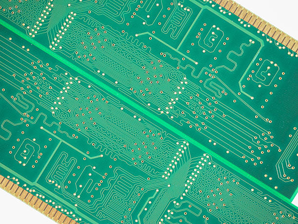
Manufacturing high-reliability 5G PCBs is not based on a single manufacturing step. Reliability is the result of coordinated control across the entire product lifecycle.
From material selection and circuit fabrication to testing and production management, every stage can influence final performance. PCB manufacturers therefore need to integrate engineering review, manufacturing process control, inspection, testing, and traceability into a unified quality system.
For projects requiring scalable production, high-volume PCB assembly can support the transition from validated designs to larger-scale manufacturing while maintaining production consistency.
Conclusion
Manufacturing a high-reliability 5G Base Station PCB requires four fundamental principles: precise material selection, strict process control, comprehensive testing, and standardized production management.
The right materials establish the foundation for environmental and electrical reliability. Precise manufacturing processes reduce defects and maintain dimensional and electrical consistency. Rigorous testing helps identify potential reliability risks before deployment. Finally, standardized production management and traceability help maintain consistent quality across batches.
By integrating these elements into a comprehensive manufacturing strategy, PCB manufacturers can produce boards capable of supporting stable high-frequency communication and long-term operation in demanding 5G base station environments.