How Strict Testing Ensures Long High-Speed High-Frequency PCB
PCB lifespan directly affects the reliability, maintenance requirements, and total cost of ownership of end equipment. Whether used in 5G base stations, industrial control systems, or high-end test instruments, premature PCB performance degradation or failure can result in equipment downtime and potentially trigger additional system-level problems.
Rigorous testing is therefore an essential part of ensuring long-term PCB reliability. From incoming material inspection to process validation and final product verification, systematic testing helps identify potential weaknesses, verify durability, and reduce the risk of premature failure.
For a High-Speed High-Frequency PCB, lifespan protection can be evaluated from four key perspectives: material characteristics, manufacturing process reliability, finished-product performance, and application compatibility.
1. Material Characteristic Verification: Establishing a Reliable Foundation
The service life of a high-speed, high-frequency PCB is closely related to the durability and stability of its raw materials. If the substrate, copper foil, solder mask, or other materials have inherent weaknesses, even a highly controlled manufacturing process may not guarantee long-term stability.
Material testing at the incoming stage can therefore help identify potential problems before production begins.
1.1 Substrate Environmental Aging Testing
High-speed and high-frequency PCBs may operate under changing temperatures and humidity conditions. If the substrate has insufficient aging resistance, long-term exposure to environmental stress may cause changes in dielectric properties or reductions in mechanical strength.
During testing, substrate samples can be exposed to simulated operating environments, such as cyclic temperature and humidity conditions. After a defined test period, key parameters such as dielectric constant, dissipation factor, and mechanical strength can be evaluated.
If these parameters remain within the required limits, the material demonstrates good resistance to environmental aging. Significant changes may indicate that a more durable substrate material should be considered.
1.2 Copper Foil Adhesion Durability Testing
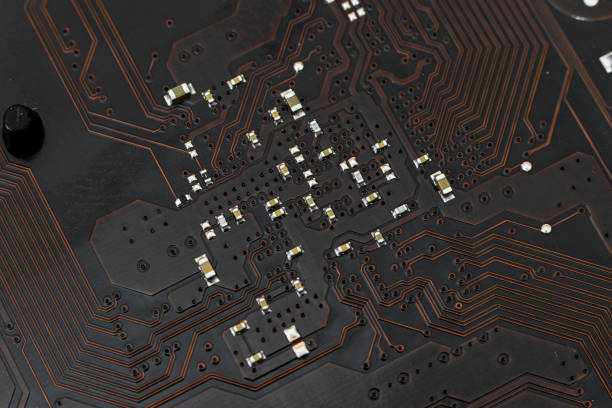
Copper foil is a critical conductor for signal transmission, and its adhesion to the substrate directly affects PCB reliability.
Insufficient adhesion may allow copper traces to separate from the substrate after prolonged exposure to vibration or temperature changes, potentially resulting in open circuits.
Peel testing can be used to evaluate the bonding strength between copper foil and the substrate. Samples can also undergo repeated environmental cycles before adhesion is tested again. This approach helps determine whether the copper-substrate bond remains stable after long-term environmental exposure.
1.3 Solder Mask Chemical Resistance Testing
The solder mask provides electrical insulation while helping protect copper circuitry from external contaminants and chemical exposure.
If the solder mask has poor chemical resistance, prolonged exposure may cause discoloration, blistering, cracking, or peeling. Once the protective layer deteriorates, exposed circuitry may become more vulnerable to corrosion and other forms of damage.
Testing can involve exposing solder-mask-coated PCB samples to chemicals representative of the intended application environment. After exposure, the surface should be examined for visible deterioration, while electrical performance can also be evaluated to determine whether the protective layer continues to function effectively.
2. Process Reliability Testing: Identifying Manufacturing-Related Risks
High-quality materials alone cannot guarantee a long PCB lifespan. Manufacturing defects such as insufficient lamination, etching residue, or uneven surface finishing can create hidden reliability risks.
For this reason, process-level testing is an important component of PCB Quality Control.
2.1 Interlayer Bonding Strength Testing
Lamination is a critical process for building multilayer PCBs into a unified structure. If interlayer bonding is insufficient, temperature cycling, vibration, and mechanical stress may eventually cause delamination.
Peel or bonding-strength testing can be performed on laminated PCB samples to verify that interlayer adhesion meets the required criteria.
Samples can also be exposed to elevated-temperature conditions for a specified period and then inspected for bubbles, separation, or other signs of delamination. These tests help confirm that the lamination process can maintain structural integrity over time.
For manufacturers looking to establish a controlled production process, GOPCBA also provides comprehensive PCB Manufacturing Services covering PCB fabrication from prototypes through production.
2.2 Trace Edge Integrity Testing
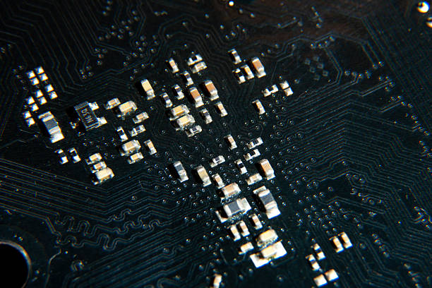
Defects introduced during etching can result in burrs, residual copper, or irregular trace edges. These issues may affect electrical performance and potentially create localized electrical or thermal stress during long-term operation.
High-magnification inspection can be used to examine trace edges for irregularities and residual material.
Long-term electrical testing can also help identify abnormal temperature increases or other performance changes associated with problematic trace areas. Precise etching control and effective inspection help minimize manufacturing-related reliability risks.
2.3 Surface Finish Uniformity and Wear Resistance Testing
Surface finishes such as ENIG and OSP play important roles in oxidation protection, solderability, and connection reliability.
Uneven surface finish thickness can create weak areas that are more susceptible to oxidation, while insufficient wear resistance may cause deterioration during assembly, insertion, or repeated mechanical contact.
Testing can evaluate surface finish thickness distribution and use simulated friction or insertion cycles to assess wear resistance. This helps determine whether the surface finish can continue protecting the underlying circuitry throughout the intended service period.
GOPCBA integrates PCB fabrication and assembly capabilities, allowing customers to coordinate board manufacturing with downstream production requirements through its Turnkey PCB Assembly Services.
3. Finished Product Verification: Evaluating Long-Term Performance
After materials and manufacturing processes have been validated, the finished PCB should undergo comprehensive testing to determine whether the complete product can maintain stable performance over an extended operating period.
3.1 Long-Term Signal Transmission Stability Testing
The primary function of a high-speed, high-frequency PCB is to transmit signals reliably. A PCB may remain physically intact while its electrical performance gradually deteriorates.
Finished PCBs can therefore be connected to a simulated operating system and subjected to extended operation. During testing, parameters such as signal loss and interference can be monitored periodically.
If these parameters remain stable throughout the test period, the PCB demonstrates good long-term signal transmission stability. If performance degradation occurs, the material and manufacturing processes should be reviewed to identify the underlying cause.
For prototype products requiring early-stage validation, Prototype PCB Assembly can help bring prototype boards into the assembly and testing stage before larger-scale production.
3.2 Structural Fatigue Testing
PCBs installed inside electronic equipment may experience continuous vibration and mechanical stress. Over time, repeated stress can contribute to trace cracking, substrate damage, or other structural failures.
Periodic mechanical stress can be applied to finished PCB samples to simulate long-term operating conditions. After a defined number of cycles, the board should be inspected for structural damage while electrical performance is also checked.
This combined evaluation helps determine whether the PCB can withstand repeated mechanical stress without compromising electrical functionality.
3.3 Long-Term Electrical Conductivity Testing
The electrical conductivity of PCB traces can deteriorate over time due to oxidation, connection problems, or other manufacturing and environmental factors.
Critical circuits can be subjected to continuous electrical loading while their resistance is monitored at regular intervals.
Stable resistance indicates that the conductive paths remain reliable. A significant increase in resistance may indicate oxidation, poor contact, or process-related defects and should trigger further investigation.
For larger production requirements, High-Volume PCB Assembly can provide a production path after prototype and validation stages have been completed.
4. Application Compatibility Testing: Matching the PCB to Its Operating Environment
Different electronic products expose PCBs to different operating temperatures, mechanical stresses, electrical loads, and surrounding components.
Even if a PCB performs well under laboratory conditions, insufficient compatibility with the final application environment can still shorten its service life.
4.1 Thermal Compatibility with the Equipment Cooling System
High-speed and high-frequency PCBs generate heat during operation. If the PCB does not work effectively with the equipment’s thermal management system, excessive local temperatures may accelerate material aging and circuit degradation.
The PCB can be installed in the target equipment and operated under simulated working loads. Temperature distribution across critical areas should then be monitored.
If temperatures remain within acceptable limits, the PCB demonstrates good thermal compatibility with the system. If localized hot spots appear, the PCB position, thermal design, or equipment cooling solution may need to be optimized.
4.2 Compatibility with Surrounding Components
A PCB must operate together with components such as ICs, connectors, power devices, and other electronic modules.
Poor compatibility can result in increased signal interference, abnormal current distribution, or localized temperature increases. Over time, these problems may accelerate aging of both the PCB and surrounding components.
Testing should therefore evaluate the PCB together with the major components in a simulated operating environment. Signal integrity, current distribution, and temperature should be monitored to verify that the complete system operates normally.
5. Building a Full-Process PCB Reliability Testing System
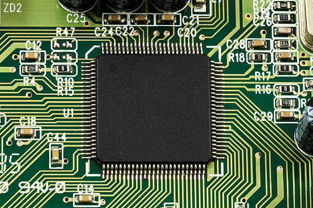
Ensuring a long PCB Lifespan cannot rely on a single test performed at the end of production. A more effective approach is to establish a complete testing loop covering materials, manufacturing processes, finished products, and actual application conditions.
The four stages work together:
- Material testing identifies weaknesses in substrates, copper foil, solder mask, and other materials.
- Process testing helps identify manufacturing defects such as delamination, trace irregularities, and surface finish problems.
- Finished-product testing evaluates long-term electrical and mechanical performance.
- Application testing verifies that the PCB can operate reliably under actual thermal, electrical, mechanical, and system-level conditions.
This layered approach allows potential reliability problems to be identified as early as possible rather than after the PCB has already entered the customer’s equipment.
6. Why Testing Is Critical to PCB Manufacturing Quality
As high-speed and high-frequency electronics continue to expand into communications, industrial control, computing, automotive electronics, and other demanding applications, PCB reliability requirements are becoming increasingly stringent.
Testing should therefore be integrated into the overall PCB Manufacturing process rather than treated as an isolated final inspection step.
A comprehensive reliability strategy can combine incoming material verification, process monitoring, electrical testing, mechanical testing, environmental testing, and application-level validation. The exact test methods and acceptance criteria should be selected according to the PCB structure, materials, operating environment, electrical requirements, and end application.
With increasingly complex electronic systems, future reliability programs will need to simulate more demanding operating conditions and adopt more precise inspection technologies. By continuously improving testing methods and integrating them throughout the manufacturing process, PCB manufacturers can provide stronger protection against premature failure and help electronic equipment achieve greater stability and durability.
Conclusion
Strict testing is one of the key foundations for improving PCB reliability and extending product service life.
From material selection and process validation to finished-product verification and application compatibility testing, each stage provides another opportunity to identify hidden risks and prevent premature failure.
For high-speed and high-frequency applications in particular, a systematic testing strategy can help ensure that PCB materials, manufacturing processes, electrical performance, mechanical structure, and application conditions work together reliably.
By integrating rigorous testing with disciplined manufacturing and quality management, PCB suppliers can build a stronger reliability foundation and provide customers with boards capable of supporting long-term electronic system operation.