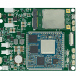


What Is EMI in PCB?
Electromagnetic Interference (EMI) in PCB design refers to unwanted electromagnetic noise that disrupts signal integrity and affects circuit performance. EMI can either be emitted from your PCB or received from external sources.
In high-speed and RF designs, poor EMI control can lead to:
- Signal distortion
- Data errors
- Regulatory compliance failure (FCC, CE)
- Product malfunction
Why EMI Happens in PCBs
Before solving EMI issues, it’s important to understand the root causes:
- High-speed signal switching (high dV/dt and dI/dt)
- Poor grounding design
- Long signal traces acting as antennas
- Impedance mismatch and reflections
- Inadequate shielding
- Power supply noise
👉 EMI is essentially an uncontrolled electromagnetic energy problem.
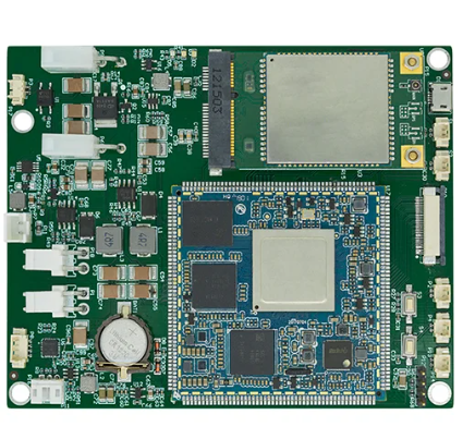
How to Reduce EMI in PCB Design
1. Use a Solid Ground Plane
A continuous ground plane is the foundation of EMI control.
✔ Reduces loop area
✔ Provides low-impedance return path
✔ Minimizes radiation
Best Practice:
- Avoid split ground planes
- Use multi-layer PCB (4-layer or more)
2. Minimize Loop Area
Large current loops act like antennas and radiate noise.
✔ Keep signal and return paths close
✔ Route high-speed signals over ground plane
👉 Smaller loop = less EMI radiation
3. Control Signal Routing
Poor routing is a major EMI source.
Key rules:
- Avoid sharp 90° corners (use 45° or arcs)
- Keep high-speed traces short
- Separate noisy and sensitive signals
- Avoid routing over gaps in ground
4. Use Proper Decoupling Capacitors
Decoupling capacitors suppress power noise.
✔ Place capacitors close to IC power pins
✔ Use multiple values (e.g., 0.1µF + 1µF)
✔ Minimize trace length to ground
5. Implement Controlled Impedance
Impedance mismatch leads to reflections and EMI.
✔ Design for 50Ω or 100Ω differential where required
✔ Maintain consistent trace geometry
✔ Avoid impedance discontinuities
6. Add Shielding and Grounding Techniques
Shielding prevents EMI leakage.
✔ Use metal shielding enclosures
✔ Ground shielding properly
✔ Use guard traces around sensitive signals
7. Optimize Power Distribution
Power noise is a major EMI contributor.
✔ Use power planes instead of long traces
✔ Add bulk capacitors for stability
✔ Separate analog and digital power
8. Use Filtering Components
Filters help suppress unwanted frequencies.
✔ Ferrite beads for high-frequency noise
✔ LC filters for power lines
✔ EMI filters at connectors
9. Reduce Via and Layer Transitions
Each via introduces impedance discontinuity.
✔ Minimize unnecessary vias
✔ Avoid stubs
✔ Use proper via design
10. Follow Proper PCB Stackup Design
A well-designed stackup improves EMI performance.
Example 4-layer stackup:
- Top: Signal
- Inner 1: Ground
- Inner 2: Power
- Bottom: Signal
✔ Keeps signals close to reference planes
✔ Reduces radiation
Quick EMI Reduction Checklist
✔ Continuous ground plane
✔ Short, direct signal routing
✔ Proper decoupling
✔ Controlled impedance
✔ Shielding where necessary
✔ Clean power distribution
Why EMI Control Matters
Ignoring EMI can result in:
- Failed compliance testing (FCC/CE)
- Product redesign costs
- Delayed time to market
- Customer complaints
👉 Good EMI design = lower risk + higher product reliability
Need Help Reducing EMI in Your PCB?
We provide:
- High-speed PCB design support
- EMI/EMC optimization
- Controlled impedance PCB manufacturing
- RF and multilayer PCB assembly
👉 Contact us today to improve your PCB performance and pass EMI compliance with confidence.