Industrial PCB Prototype Manufacturing: Process, Cost & Lead Time Complete Guide
In industrial automation, industrial control, power equipment, robotics, instrumentation, energy systems, and industrial IoT, PCBs often need to operate reliably over long periods while enduring temperature variations, mechanical vibration, electrical stress, and harsh industrial environments. Therefore, before moving to volume production, industrial PCB prototyping and design verification are essential.
Industrial PCB prototype manufacturing is not just about making a few sample boards; it is a critical step to validate PCB design, electrical performance, thermal behavior, mechanical fit, component assembly, and manufacturing feasibility.
For OEMs, R&D teams, and industrial equipment manufacturers, industrial PCB prototyping helps identify design and manufacturing issues before mass production, reducing later modification costs and shortening product development cycles.
This article systematically covers the industrial PCB prototyping process, cost, lead time, material selection, quality inspection, and how to choose a prototype manufacturer – helping engineers and procurement professionals efficiently transition from PCB design to volume production.
What Is Industrial PCB Prototyping?
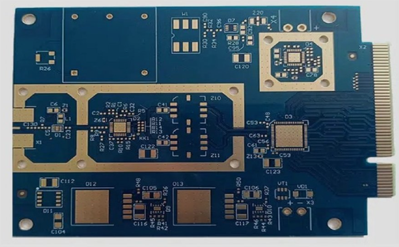
Industrial PCB prototyping refers to manufacturing a small quantity of PCB samples based on design files before full-scale production, for design verification, functional testing, and production feasibility validation. Compared to consumer PCBs, industrial PCBs typically have higher reliability requirements.
Depending on the application, industrial PCBs may require high-Tg FR-4, heavy copper, multilayer, high-frequency, metal-core, HDI, high-voltage, fine-line, impedance-controlled, high-reliability designs, high-density component placement, and thermal management. Thus, industrial PCB prototyping is not simply about “making a working PCB” – it is about validating that the entire design meets real-world product requirements. Catching design issues early through prototyping avoids costly rework, scrap, and design changes after production has started.
Why Do Industrial Electronics Need PCB Prototyping?
Industrial equipment typically has long product lifecycles and demands high stability and reliability. Failures in industrial controllers, PLCs, drives, power modules, robot control boards, or sensors can cause entire systems to shut down, resulting in significant financial losses.
Industrial PCB prototyping helps engineers verify several aspects:
2.1 Verify Electrical Performance
Prototypes allow testing of signal integrity, power integrity, voltage stability, current-carrying capacity, EMI/EMC performance, high-frequency signal transmission, circuit noise, and power conversion efficiency – especially critical for high-speed, high-voltage, or high-current industrial electronics.
2.2 Verify Thermal Performance
Many industrial devices run continuously, and power components generate significant heat. Prototyping enables verification of component operating temperatures, PCB temperature distribution, copper heat dissipation, thermal pad design, thermal vias, heatsink attachment, and metal-core thermal performance. If results are unsatisfactory, layout, copper weight, thermal structures, and materials can be adjusted before production.
2.3 Verify Mechanical Fit
Industrial PCB prototypes must match product enclosures and mechanical structures. Key checks include PCB dimensions, mounting hole positions, connector locations, component heights, board outline, clearance, cable routing, and connector interference.
2.4 Verify Manufacturability (DFM)
A design that works in theory may not be suitable for stable volume production. Prototyping reveals issues such as trace/space violations, insufficient annular rings, too-small vias, solder mask clearance problems, component spacing, via design flaws, poor stack-up, uneven copper distribution, and SMT soldering difficulties. Thus, prototyping is a key DFM validation step.
Industrial PCB Prototyping Manufacturing Process
A professional industrial PCB prototyping service typically includes engineering review, fabrication, assembly, and testing.
Step 1: PCB Design File Review
The manufacturer reviews Gerber files, NC drill files, PCB mechanical drawings, stack-up, BOM, pick-and-place files, and special process requirements. DFM checks include minimum trace/space, minimum hole size, annular ring, copper weight, board thickness, solder mask spacing, silkscreen clearance, hole accuracy, layer registration, and outline tolerances.
Step 2: Material Selection
Materials are chosen based on electrical, thermal, mechanical, and reliability needs. Common options: FR-4, high-Tg FR-4, high-frequency laminates, low-loss materials, metal-core (aluminum), polyimide, ceramic. For standard industrial control, FR-4 is often sufficient; high-Tg for high-temperature environments; high-frequency materials for RF and high-speed designs.
Step 3: PCB Fabrication
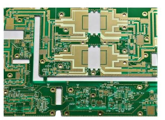
The typical manufacturing flow includes: material cutting, inner-layer imaging, inner-layer etching, lamination, mechanical or laser drilling, desmear, electroless copper, copper electroplating, outer-layer imaging, etching, solder mask, surface finish, silkscreen, routing, electrical testing, and final inspection. Special processes vary for HDI (laser microvias), heavy copper (thicker plating/etching), etc.
Common Materials for Industrial PCB Prototypes
- FR-4: Widely used for industrial control, PLC, automation, instrumentation, and general electronic control systems – offers good insulation, mechanical strength, mature processing, stable supply, and low cost.
- High-Tg FR-4: Better thermal and dimensional stability for industrial power, motor controllers, automation, and high-temperature electronics.
- Heavy Copper PCB: For high-current applications like motor drives, power converters, industrial power supplies, battery management, and energy storage – improves current capacity and heat dissipation but increases cost and complexity.
- Metal-Core PCB (e.g., aluminum): For high-power LED, power modules, and industrial lighting – excellent heat dissipation.
- High-Frequency PCB: For industrial wireless, RF, and high-speed data – low dielectric loss and stable Dk, typically costlier than FR-4.
Factors Affecting Industrial PCB Prototype Cost
- Layer count: 2-layer < 4-layer < 6-layer and above.
- PCB size: Larger boards consume more material and may reduce panel utilization.
- Base material: High-Tg, high-frequency, ceramic, or metal-core cost more than standard FR-4.
- Copper weight: 2oz, 3oz, 4oz, or heavier increase cost.
- Trace/space precision: Finer lines require tighter process control and higher cost.
- Via technology: Blind, buried, microvias, and HDI add cost.
- Surface finish: ENIG, hard gold, etc., are more expensive than HASL or OSP.
- Quantity: Engineering and setup costs are amortized over fewer boards for small batches, raising per-unit cost.
- PCB assembly (PCBA): If assembly is required, component count, SMT/DIP, BGA/QFN, procurement, and testing add significant cost.
2026 Industrial PCB Prototype Cost Reference
Prices vary widely. The following are budget estimates (USD) for small-batch prototyping in 2026:
- 2-layer FR-4: ~$30–$150
- 4-layer: ~$60–$250
- 6-layer: ~$120–$400
- 8+ layers: ~$200–$600+
- HDI: ~$150–$800+
- Heavy copper: ~$100–$500+
- High-frequency: ~$150–$800+
- Industrial PCBA prototype: ~$100–$1,000+, depending on BOM and assembly complexity
These are estimates only. Actual quotes depend on size, layer count, material, copper weight, trace/space, hole size, finish, quantity, special processes, components, assembly, testing, and delivery. For an accurate quote, submit Gerber, stack-up, BOM, quantity, and target lead time.
Industrial PCB Prototype Lead Time
Typical manufacturing lead times:
- Simple 2-layer: 3–5 working days
- 4-layer: 4–7 days
- 6-layer: 5–8 days
- 8+ layers: 7–12 days
- HDI or special materials: 7–15+ days
If PCBA is required, add procurement and assembly time. A complete prototype (PCB + assembly + test) may take 7–20 working days. Delays can occur due to incomplete Gerber, design changes, BOM errors, component shortages, special material procurement, complex stack-up, HDI, BGA assembly, special testing, or customer approval lag. Ensure complete and accurate design files to minimize lead time.
Industrial PCB Prototype vs. Production PCB
Prototyping focuses on rapid validation, finding design flaws, verifying electrical/mechanical/assembly performance and reliability. Production focuses on unit cost, efficiency, yield, process stability, batch consistency, supply chain, and long-term delivery. A good prototype manufacturer should also support volume production to ensure a smooth transition.
How to Reduce Industrial PCB Prototype Cost and Lead Time
- Simplify design: Avoid unnecessary HDI or fancy structures if conventional through-hole and multilayer work.
- Choose materials wisely: Use standard FR-4 unless high temperature, high frequency, or high power demands special materials.
- Provide complete data: Gerber, drill, BOM, pick-and-place, mechanical drawings, stack-up, and special requirements – reduces back-and-forth.
- Apply DFM early: Consider trace/space, hole size, pad dimensions, component spacing, copper balance, thermal vias, and panelization during design.
- Select a manufacturer that supports both prototyping and volume production: This avoids requalification and process adjustments when scaling up.
Quality Inspection for Industrial PCB Prototypes
Visual inspection alone is insufficient. Professional manufacturers perform AOI (for trace and soldering defects), electrical testing (opens/shorts), X-Ray (for BGA/QFN hidden joints), dimensional checks (length, width, thickness, hole size/position), and surface finish inspection. Additional reliability tests may be added for high-reliability products.
How to Choose an Industrial PCB Prototype Manufacturer
Avoid comparing only the lowest price. Evaluate:
- Manufacturing capability: layer count, board thickness, copper weight, min trace/space, hole size, special materials, surface finishes, HDI, high-Tg, heavy copper.
- Engineering support: Can they identify design risks before production?
- Lead time reliability: Realistic delivery schedules.
- Quality certifications: ISO 9001, UL, RoHS, etc.
- Prototype-to-production scalability: Can they handle small-batch and high-volume runs?
- Communication efficiency: Quick and clear engineering feedback.
Key Application Areas for Industrial PCB Prototyping
- Industrial automation: PLC, controllers, I/O, motion control, robotics.
- Power electronics: industrial power supplies, inverters, motor drives, battery management, energy storage.
- Industrial IoT: data acquisition, wireless, remote monitoring, sensors, edge computing.
- Instrumentation: test/measurement equipment, sensors, data loggers.
- Renewable energy: solar, storage, charging equipment, power management.
Why Choose gopcb for Industrial PCB Prototyping?
For industrial OEMs, a professional PCB provider should offer comprehensive capabilities from prototype development to volume production. gopcb delivers PCB manufacturing and PCBA solutions tailored to industrial requirements, supporting single-sided, double-sided, multilayer, high-Tg, heavy copper, metal-core, high-frequency, HDI, rigid-flex, and PCBA assembly. By integrating engineering review, fabrication, assembly, testing, and production support within one supply chain, we reduce coordination overhead and transition risks.
Explore our services: PCB manufacturing, prototype PCB assembly, turnkey PCB assembly, low-volume PCB assembly, and high-volume PCB assembly.
For an industrial PCB prototype quote, provide Gerber, layer count, dimensions, material, copper weight, thickness, surface finish, BOM, quantity, PCBA requirements, and target lead time. We will evaluate and provide an accurate cost and schedule.
FAQ: Industrial PCB Prototyping
1. How long does industrial PCB prototyping take?
Simple 2-layer boards: 3–5 working days; complex multilayer, HDI, or special materials: 7–15+ days; with PCBA, add procurement and assembly time.
2. How much does industrial PCB prototyping cost?
Simple 2-layer FR-4 small batches: ~$30–$150; 4-layer, 6-layer, HDI, heavy copper, high-frequency can range to several hundred dollars or more. Final cost depends on specific parameters.
3. What materials are commonly used for industrial PCB prototypes?
FR-4 is most common; high-Tg FR-4, high-frequency, metal-core, ceramic, and polyimide are used for special requirements.
4. Can industrial PCB prototypes be used directly for production?
They serve as the basis, but before full production, DFM optimization, panelization, material finalization, process tuning, and parameter validation are needed.
5. What files are needed for industrial PCB prototyping?
Gerber, drill files, mechanical drawings, stack-up. For PCBA, also BOM and pick-and-place files.
6. What is the difference between PCB prototyping and production?
Prototyping focuses on design validation and testing with small quantities; production focuses on cost, yield, efficiency, consistency, and long-term delivery.
7. Is quick-turn prototyping more expensive?
Yes, expedited service typically costs more due to priority scheduling and resource allocation.
8. How can I reduce industrial PCB prototype cost?
Reduce layer count if possible, choose appropriate materials, avoid unnecessary HDI, optimize board size, provide complete data, and choose a manufacturer that supports both prototyping and volume production.
Conclusion
Industrial PCB prototyping is a vital bridge between design and volume production. Through prototypes, engineers can verify electrical performance, thermal behavior, mechanical fit, reliability, component assembly, signal integrity, and manufacturability. Cost and lead time depend on layer count, material, size, copper weight, trace/space, via technology, finish, quantity, assembly, component availability, and testing.
For typical industrial control PCBs, FR-4 and conventional multilayer designs offer good cost-effectiveness. For high-temperature, high-current, high-frequency, high-speed, or high-reliability products, high-Tg, heavy copper, high-frequency, HDI, or other special structures may be needed.
For OEMs, the ideal PCB partner should provide a complete service from DFM engineering review → prototyping → PCBA → functional testing → small-batch → high-volume production. Choosing such a partner reduces development risk, lowers supply chain switching costs, and accelerates the transition from prototype to production.
If you are looking for a professional industrial PCB prototype manufacturer or PCBA supplier, contact gopcb with your Gerber, BOM, specifications, quantity, and target lead time to receive a customized quote for your project.