LDI in PCB Fabrication: Laser Direct Imaging for Fine Lines
For decades, printed circuit patterns were transferred the way photographs were printed: a transparent film carried the image, and light passed through it onto a photosensitive coating. That approach served the industry well, but it has a physical ceiling. As line widths approach the thickness of the film itself and the packaging on top of the board becomes denser, the limits of the photographic method start to define what can be built.
Why Film Artwork Reached Its Limit
The pressure comes from several directions at once. Component integration continues to increase, and chip scale and micro ball grid array packages drive pad counts and routing density upward. Products keep getting thinner, lighter and smaller, while signals move toward higher frequencies and higher speeds. Together these trends demand finer conductors, tighter positional accuracy and better registration between layers.
Conventional film based image transfer struggles with all three. The film has its own dimensional behaviour, it stretches slightly under tension, it wears with repeated use, and contact with the resist can trap particles that print as defects. At line widths and spaces below about thirty micrometres the method approaches its practical limit, which is why direct imaging moved from an expensive curiosity to a mainstream requirement.
How Laser Direct Imaging Works
Laser direct imaging removes the film entirely. Instead of projecting through a mask, a modulated laser or laser array scans the photoresist directly, driven by the digital data from the CAM database. The pattern exists only as data until the moment it is written onto the panel, so there is nothing to align, nothing to stretch and nothing to wear out.
Because the image is generated electronically, each panel can be exposed with a slightly different transformation. The machine measures fiducials on the actual panel, calculates the scale and rotation error present in that specific piece, and corrects the pattern before exposing. That per-panel correction is the single largest source of accuracy improvement over film, and it directly addresses the registration problem that limits high layer count fabrication.
Layer-to-Layer Registration Gains
Registration is where the benefit is most measurable. A film shrinks and expands with temperature and humidity, and the same film used on a Monday may print differently on a Friday. Since the film itself defines the pattern, its errors pass straight into the copper. Direct imaging replaces that variable with a measured correction applied to a fixed digital master.
The result is that inner layer patterns can be placed against each other far more accurately, which matters most on thick, high layer count boards where a small per-layer error accumulates. Better registration also allows tighter pad-to-pad tolerances, so designs that would otherwise need extra spacing can be built as drawn. The wider topic of dimensional behaviour is covered in PCB dimensional stability and expansion.
Fine Lines Below Thirty Micrometres
Resolution improves for a simpler reason. Light passing through a film is scattered and diffracted by the film material and by the gap between film and resist. A focused laser writing directly onto the surface does not suffer that loss, so the exposed edge is sharper and the developed feature more faithful to the data.
That matters for both line width and space. Narrower traces allow higher routing density, and narrower spaces allow more conductors between component pads. Where the resist is a thin liquid coating rather than a laminated film, the two advantages compound, which is why the two technologies are often specified together. The comparison is set out in wet film versus dry film photoresist.
Effect on Process Flow and Yield
Removing the film removes a whole series of small process steps and their associated defects. There is no film generation, no film inspection, no film storage, no vacuum draw-down and no contact related scratching. Particle defects that originate from the film interface disappear, and rework becomes simpler because the exposure can be repeated from the same master.
There is also an operational gain. Because the pattern is digital, engineering changes do not require new artwork. A revised design can be exposed the same day, and different panel sizes can run back to back without setup change. That flexibility compresses the prototype cycle considerably, which is often worth more to a customer than the direct cost saving.
Cost, Throughput and Where LDI Pays
Direct imaging equipment is expensive and its throughput is lower than a conventional exposure unit running a large panel through once. It therefore pays where the requirement is genuinely fine geometry, tight registration or fast turnaround, and it is less attractive for coarse, high volume boards where film costs are amortised across a long run.
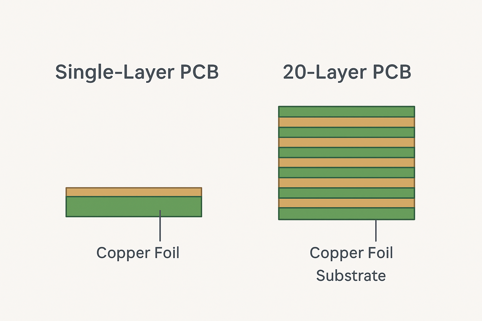
The economics also depend on yield. When a board has ten inner layers, a registration failure at layer eight wastes everything built before it, so improving accuracy at each imaging step has a multiplicative effect on the value of the panel. For demanding multilayer work, that calculation usually favours direct imaging even before the resolution advantage is considered.
Combining LDI with Inkjet and Other Tools
Direct imaging is not the only digital patterning route. Inkjet printing can deposit resist or even conductive material without any exposure step, and it is attractive for legend, for selective coating and for certain additive processes. The two techniques are complementary rather than competing, since each suits a different layer and a different resolution range.
In practice a modern shop may use direct imaging for critical layers, conventional exposure for coarse ones and inkjet for legend. What matters is that the CAM data feeding all of them is consistent, and that the tooling decisions are made when the design is released rather than when it reaches the imaging area. Related process control topics appear under copper plating defects prevention and HDI board CAM methods.
Verifying the Image Before Etching
Direct imaging shifts the verification burden rather than removing it. Because the pattern is generated from data, a data error propagates to every panel in the lot, whereas a film defect usually affects only the pieces it touches. The CAM database therefore has to be validated before the job starts, and the first panel of a run deserves a proper measurement rather than a glance.
In practice that means checking line width and space on a coupon using a calibrated measuring system, confirming registration against the target pattern with an inner layer inspection tool, and reviewing the developed image under magnification for incomplete exposure or residue. Laser energy, focus and scan linearity drift slowly, so a periodic qualification artefact is the most reliable way to confirm that the machine is still writing what the data describes. Doing this before etching keeps a systematic error from being repeated across an entire production lot.
FAQ
What line width can LDI achieve? Direct imaging is the practical route to lines and spaces below about thirty micrometres, where film based transfer becomes unreliable. The exact figure depends on resist type, copper thickness and the imaging equipment.
Does LDI remove the need for registration tolerance? No. It reduces the error contributed by the imaging step and corrects per panel distortion, but material movement, lamination and drilling still consume part of the registration budget.
Is LDI worth it for a simple two layer board? Usually not on cost alone. It pays where geometry is fine, registration is tight, layer count is high or the schedule is short enough that avoiding film generation matters.