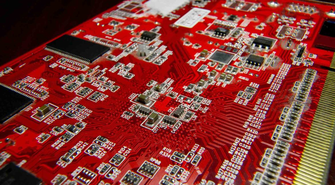
A successful low volume PCB assembly project requires more than placing components on a printed circuit board.
When products contain fine-pitch BGA, QFN, 0201 components, double-sided SMT, mixed technology, or HDI PCB structures, manufacturing quality depends on the interaction between PCB fabrication, component selection, solder paste printing, component placement, reflow, inspection, testing, and process control.
For this reason, low-volume production should be managed with the same engineering discipline as larger production runs.
Kingda provides integrated PCB manufacturing and PCB assembly services, including SMT, through-hole assembly, component procurement, inspection, testing, and turnkey manufacturing.
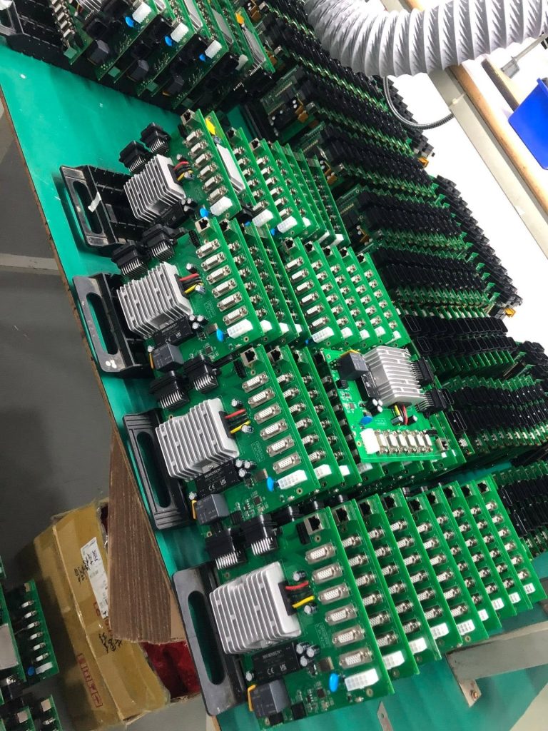
Low Volume PCB Assembly Process
A typical manufacturing workflow includes:
- Engineering data review
- PCB fabrication
- Component procurement
- Incoming inspection
- Solder paste printing
- SPI
- SMT placement
- Reflow soldering
- AOI
- X-ray inspection where required
- THT assembly
- Electrical testing
- Functional testing
- Final inspection
- Packaging and shipment
Each stage contributes to final PCBA quality.
SMT PCB Assembly
SMT PCB assembly is the primary manufacturing technology for many modern electronic products.
Surface-mount technology allows components to be placed directly onto PCB pads, enabling compact layouts and high component density.
Modern PCB assemblies may include:
- 01005 components
- 0201 components
- QFN
- LGA
- BGA
- Fine-pitch ICs
- Connectors
- Power devices
- RF components
Kingda states that its SMT capabilities support fine-pitch components, BGA packages down to approximately 0.35 mm pitch, and passive components down to 01005, with X-ray inspection available for hidden solder joints.
These capabilities are particularly relevant for compact, high-density electronic products.
Solder Paste Printing
Solder paste printing is one of the most important stages in SMT PCB assembly.
Problems during printing can lead to:
- Insufficient solder
- Excessive solder
- Solder bridges
- Component movement
- Tombstoning
- Open joints
- BGA defects
The process depends on:
- Stencil thickness
- Aperture geometry
- Solder paste properties
- PCB support
- Printing pressure
- Printing speed
- Alignment accuracy
For fine-pitch components, stencil design becomes increasingly important.
QFN thermal pads, for example, should generally not be treated as one large uninterrupted stencil opening. A carefully designed aperture pattern can help control solder volume and reduce excessive voiding or floating.
SPI Inspection
Solder Paste Inspection (SPI) evaluates the quality of the solder paste deposition before component placement and reflow.
Typical parameters include:
- Paste volume
- Paste height
- Paste area
- Paste position
- Offset
SPI provides early feedback.
Instead of waiting until after reflow to discover solder-related defects, manufacturers can identify printing problems while the board is still in the early assembly stage.
Precision SMT Placement
Component placement must account for:
- Package size
- Pad geometry
- Component orientation
- Fiducial accuracy
- PCB warpage
- Placement tolerance
- Component pickup characteristics
Fine-pitch BGA and small passive components require precise control.
For low volume PCB assembly, this is particularly important because frequent product changeovers can introduce additional setup risks.
Controlled programs and first-article verification help ensure that the correct placement data is used for every production revision.
Reflow Soldering
Reflow soldering converts printed solder paste into permanent solder joints.
A reflow profile should be developed according to:
- Solder paste specifications
- PCB thermal mass
- Component temperature limits
- Board copper distribution
- Component package mix
- Required peak temperature
- Time above liquidus
The objective is not simply to achieve a high temperature.
The entire board should reach an appropriate thermal profile while respecting component and material limits.
Complex PCBs may require multiple thermocouple locations to understand temperature differences between heavy copper areas, BGA regions, small components, and thermal pads.
BGA PCB Assembly
BGA PCB assembly presents additional inspection and process-control challenges because many solder joints are hidden beneath the package.
Potential defects include:
- Open solder joints
- Bridges
- Voiding
- Misalignment
- Insufficient solder
- Head-in-pillow defects
Visual inspection alone cannot provide complete visibility into BGA solder joints.
Therefore, X-ray inspection is often used for BGA assemblies.
Kingda provides X-ray inspection as part of its PCB assembly quality-control capabilities.
QFN Assembly
QFN packages provide excellent electrical and thermal performance while occupying relatively little PCB area.
However, the exposed thermal pad can make soldering more difficult.
Common problems include:
- Excessive voiding
- Floating components
- Uneven solder distribution
- Poor thermal transfer
- Hidden solder defects
Stencil aperture design, solder volume, pad design, and reflow profile all influence QFN assembly quality.
For demanding applications, X-ray inspection can be used to evaluate hidden solder connections.
Through-Hole PCB Assembly
Not every product can rely entirely on SMT.
Through-hole PCB assembly remains important for:
- Large connectors
- Power components
- Mechanical interfaces
- High-stress components
- Industrial equipment
- Components requiring additional mechanical strength
Kingda supports both manual and automated through-hole assembly as well as wave and selective soldering processes depending on product requirements.
A mixed-technology product may therefore combine:
SMT + THT + selective soldering + manual assembly + testing
within a single manufacturing project.
HDI PCB Assembly
High-density products may require HDI PCB technology.
HDI can improve routing density through:
- Laser microvias
- Sequential lamination
- Fine-line circuitry
- Via-in-pad structures
- High-density BGA fanout
HDI is particularly useful for compact electronic products where conventional through-hole vias cannot provide sufficient routing space.
However, HDI also introduces additional manufacturing requirements.
These may include:
- Laser drilling
- Sequential lamination
- Microvia plating
- Via filling
- Registration control
- Stack-up management
- Impedance control
Kingda’s PCB manufacturing capabilities include HDI PCB, high-frequency PCB, high-speed PCB, flexible PCB, rigid-flex PCB, multilayer PCB, blind vias, buried vias, plugged vias, and custom stack-ups.
This integrated PCB fabrication capability can be valuable for low-volume projects involving complex board structures.
AOI Inspection
Automated Optical Inspection (AOI) is commonly used after reflow.
AOI can identify visible defects such as:
- Missing components
- Incorrect components
- Component misalignment
- Reversed components
- Solder bridges
- Visible solder defects
AOI provides repeatable inspection across the production batch.
For low-volume production, it can also provide useful process feedback without relying entirely on manual inspection.
X-Ray Inspection
X-ray inspection provides visibility into hidden solder joints.
It is especially useful for:
- BGA
- QFN
- LGA
- Bottom-terminated components
- Hidden connections
Typical inspection targets include:
- Voiding
- Opens
- Bridges
- Insufficient solder
- Misalignment
For complex assemblies, combining SPI + AOI + X-ray creates stronger process visibility than relying on a single inspection method.
PCB Assembly Testing
Inspection and testing answer different questions.
Inspection asks:
Does the assembly appear to be manufactured correctly?
Testing asks:
Does the assembly electrically and functionally perform as required?
A comprehensive PCBA testing strategy may include:
Visual Inspection
Used to identify:
- Missing components
- Incorrect orientation
- Mechanical damage
- Soldering problems
Flying Probe Testing
Flying probe testing can check electrical connections without requiring a dedicated ICT fixture.
It can be useful for prototypes and low-volume production where fixture cost needs to be controlled.
ICT
In-Circuit Testing (ICT) can evaluate electrical networks and selected component characteristics.
It is particularly useful when the product has a stable design and repeat production.
Functional Testing
Functional testing verifies the actual operating behavior of the completed PCBA.
Depending on the product, this may include:
- Power-up testing
- Communication testing
- Sensor verification
- Display testing
- Motor control
- Network communication
- RF testing
- System-level operation
Kingda supports AOI, X-ray, electrical testing, ICT, and functional testing according to project requirements.
Quality Control for Low Volume PCB Assembly
Low production volume does not mean reduced quality requirements.
A controlled quality system may include:
Incoming Material → SMT Process → Inspection → THT → Electrical Test → Functional Test → Final Inspection → Shipment
Kingda states that its manufacturing process incorporates inspection and testing throughout production and maintains product traceability through its ERP system.
This helps connect production records with individual manufacturing orders and supports product lifecycle management.
PCB Assembly Traceability
Traceability becomes increasingly important as products become more complex.
A traceability system may record:
- PCB lot
- Component lot
- Production order
- Manufacturing date
- Equipment
- Inspection results
- Test results
- Rework history
- Engineering revision
For a product experiencing a field failure, traceability can help engineers determine whether the issue is related to:
- A specific component lot
- A PCB batch
- A production revision
- A process condition
- A test failure
Kingda’s ERP-based manufacturing system supports whole-process traceability as part of its quality and production management approach.
PCB Assembly Quality Standards
Depending on the product and customer requirements, electronic manufacturing may reference standards such as:
- IPC-A-610
- IPC J-STD-001
- IPC-6012
- IPC-7711/7721
- ISO 9001
- ISO 13485
- IATF 16949
The applicable standard and acceptance class should be clearly defined before production.
Kingda states that it operates under ISO 9001, ISO 13485, and IATF 16949 quality management systems, supporting applications including general electronics, medical electronics, and automotive-related products.
Why One-Stop PCB Manufacturing Matters
A major advantage of working with an integrated PCB manufacturing and assembly supplier is the ability to coordinate multiple manufacturing stages through one organization.
Instead of separately managing:
PCB Supplier → Component Supplier → SMT Factory → Testing Supplier
customers can work with one manufacturing partner for:
PCB Design → PCB Manufacturing → Component Procurement → SMT → THT → Testing → Final Assembly
Kingda provides this one-stop manufacturing model.
This can simplify:
- Engineering communication
- Procurement
- Production scheduling
- Quality control
- Revision management
- Logistics
- Technical problem solving
Kingda’s Manufacturing Advantages
Integrated PCB and PCBA Capabilities
Kingda combines PCB fabrication and assembly, supporting standard multilayer boards as well as HDI, flexible, rigid-flex, high-frequency, and high-speed PCB technologies.
Flexible SMT and THT Assembly
The manufacturing system supports SMT, through-hole, and mixed-technology assembly for prototype, low-volume, and higher-volume requirements.
Advanced Inspection
Kingda supports:
- SPI
- AOI
- X-ray
- Electrical testing
- ICT
- Functional testing
This allows inspection and testing to be matched to the complexity and risk of each product.
Engineering Support
DFM and DFA engineering support helps customers identify manufacturing risks before production begins.
Global Component Sourcing
Kingda provides component procurement through its supplier network, supporting turnkey and partial-turnkey production models.
Fast Response
Kingda promotes 24/7 sales and technical support and rapid response for customer projects, which is particularly valuable for prototype and low-volume projects where engineering changes can occur frequently.
How to Improve Low Volume PCB Assembly Yield
Improving yield starts before the SMT machine begins production.
The most effective approach is to control the entire process:
Step 1: Improve PCB Design
Use DFM/DFA review to identify:
- Insufficient spacing
- Difficult-to-manufacture vias
- Poor component orientation
- Inadequate test points
- Stencil problems
Step 2: Control Components
Verify:
- Manufacturer part numbers
- Package types
- Lifecycle status
- Approved alternatives
- Moisture sensitivity
Step 3: Optimize Stencil Design
Pay special attention to:
- Fine-pitch ICs
- QFN thermal pads
- BGA
- 0201/01005 components
Step 4: Validate Reflow
Measure the board temperature at representative locations and verify the profile against solder paste and component requirements.
Step 5: Inspect Early
Use SPI and first-article inspection to detect process problems before the entire lot is completed.
Step 6: Test the Finished PCBA
Combine electrical and functional testing according to the product’s actual requirements.
Conclusion
A reliable low volume PCB assembly process requires the same fundamental discipline as larger-scale manufacturing.
The key elements include:
- Accurate PCB fabrication
- Reliable component sourcing
- Controlled SMT placement
- Optimized soldering
- THT assembly where required
- SPI
- AOI
- X-ray
- Electrical testing
- Functional testing
- Traceability
- Revision control
- Engineering support
For complex products, the quality of the final PCBA depends on how well these individual processes are integrated.
Kingda’s one-stop manufacturing model combines PCB manufacturing, component procurement, SMT, THT, testing, DFM/DFA, and finished-product services, allowing customers to manage development and production through a single manufacturing partner.
From a simple prototype to a complex HDI assembly, the objective remains the same: build a reliable electronic product with controlled quality, predictable manufacturing, and an efficient path from engineering to production.